This chapter describes how to
examine a frozen CHALLENGE, POWER CHALLENGE, Onyx, or POWER Onyx system
determine whether a problem is caused by hardware or software
determine where hardware problems occur in a system
use various diagnostic tools and techniques for manufacturing and field service technicians
A scenario of a frozen system demonstrates how to use the debugging tools.
When a system is frozen, it is either hung or the kernel has panicked. It is important to determine which case has occurred in the system you are diagnosing because the procedures for fixing a hang are different from those for fixing a kernel panic.
 | Note: The best way to find a system hang or panic is to examine it while it is still frozen. If the system is at a customer site, this may not be possible, since the customer may already have reset or rebooted the system. Encourage a customer who is experiencing hangs or panics to leave the system frozen until you can examine it. If a customer must reboot a system before you can examine it, ask the customer to first generate a core dump using a nonmaskable interrupt from the System Controller. (See Section 4.5.2, "Key Switch in the Manager Position.") If the customer does this when the system hangs, you can later examine the core file for clues to the cause of the problem. |
A system can be frozen six basic ways, due to either hardware or software problems, as shown in Table 2-1:
Table 2-1. Likely Causes of Common System Problems
System Condition | Likely Cause |
|---|---|
The kernel is under such a heavy disk swapping load that no processes can run.
| Software problem or insufficient system resources, such as memory and swap space. |
The kernel is running out of a software resource and cannot perform normal process scheduling.
| Insufficient system resources, such as kernel buffers, memory, and swap space. |
One or a few processes are hung, but other processes are running fine.
| Software problem. |
No processes are running, but the kernel is still ticking at interrupt level.
| Software problem. |
Processors are stuck spinning in the kernel; interrupts are also blocked.
| Software problem. |
One or more processors are not executing instructions normally.
| Hardware problem. |
Only the last condition indicates a hardware error. Deal with the other cases by gathering appropriate information and filing a bug report.
If the system is still hung, follow these steps to help isolate the problem:
Examine the serial port console, if available. Do the last messages look like normal activity, or is the serial port console showing a panic or sitting at a DBG: prompt?
If there are no signs of a kernel panic or crash, type a few characters on the serial console and see if they echo. If they echo, then the kernel is still ticking at interrupt level; this is probably a software bug.
Corrective action: Generate a nonmaskable interrupt (NMI) core dump and file a bug report. See Section 4.5.2, "Key Switch in the Manager Position," for the System Controller menu selections to create an NMI core dump.
Look at the power meter and open the first drive tray to see the disk LEDs. Notice if the power meter is moving. (It updates about once per second). See if disk LEDs are blinking.
Note: Distinguish between an LED that is stuck on "on" and one that is blinking. Disk LEDs can sometimes blink very rapidly and might appear at first to be stuck on. If either the power meter or the disk LEDs show activity, some processes are still running on the system. A disk with an LED almost constantly on could indicate heavy swapping activity, causing what looks like a hang. If the system exhibits these symptoms, suspect a software problem
Corrective action: Generate an NMI core dump and file a bug report.
If the system is on a network, log in to another host and try to ping the hung system by using the command /usr/etc/ping. If ping indicates 100 percent packet loss, then the kernel is not ticking at interrupt level.
Try to log into the frozen system using rlogin. If you can log in successfully, type date at the shell prompt. Or, type ps -efl. If both of these commands run properly, the hang is a software problem.
Corrective action: Generate an NMI core dump and file a bug report.
If the date and ps commands do not run properly, proceed to the next step.
If there was no response to the serial console, power meter, drive LEDs, or logging in and running date or ps over the network, try to determine if processors are stuck spinning in the kernel. Perform a front-panel NMI.
If one NMI causes the kernel to display
PANIC: User requested vmcore dump (NMI)
then processors are responding normally. This is probably a software problem.
Corrective action: File a bug report.
If there is no response to the first NMI, then issue a second NMI.
After you issue the second NMI the bootmaster processor will try to enter the PROM power-on diagnostic monitor (POD). If POD is successfully entered, follow the procedure in Section 5.6.4, "Using POD to Examine HARDWARE ERROR STATE Messages," to see if any hardware bits are set. If any hardware bits are set, then this is probably a hardware failure.
Corrective action: Based on the HARDWARE ERROR STATE messages, swap the appropriate hardware to locate and eliminate the problem.
If no error bits are set, then it is probably a software problem.
Corrective action: File a bug report.
If there is no response to the second NMI, use the procedure in section Section 2.5.5, "Procedure to Cause a Hung System to Enter POD Mode," to try to reset into POD.
If there are no error bits set, then it is still probably a software problem, with corruption of kernel memory. Entering POD depends on a few words of memory being correct.
Corrective action: File a bug report.
| Note: One hardware problem that can look like a software problem under the guidelines in Table 2-1 is if some (but not all) processors are not executing instructions normally, but at least one CPU continues to execute. If you suspect this may be the case, see Section 2.5.4, "Using a Debug Kernel to Find System Hangs." |
If the system has already been reset or rebooted by the time you examine it, there is nothing remaining to look at. Ask the customer to allow you to examine the system the next time it hangs.
If the customer cannot wait for you to arrive after the system hangs, ask the customer to use the System Controller to issue a nonmaskable interrupt (NMI), which should create a system core dump.
If the system dumps core after the customer issues an NMI, then you should suspect a software problem, in particular with the operating system (IRIX). If the system doesn't respond, then the hardware may be at fault. If there is a hardware problem, the /var/adm/SYSLOG file may contain kernel messages preceding the hang that should be included in any bug reports.
When the IRIX kernel panics, it displays one of several error messages and then stops running purposefully. There are both hardware and software causes for kernel panics. To determine the cause of the panic, collect the messages that the kernel printed at panic time and classify them.
At panic time, messages are displayed on the system console; this is useful only if the system console is set to the serial port console. The kernel then attempts a core dump, in which the messages are stored. At boot time, the utility savecore(1M) copies the panic messages into the file /var/adm/SYSLOG and stores the core dump in a file called /var/adm/crash/vmcore.N.comp. In the actual filename, N is a number that identifies each particular core dump if there is more than one dump file in the crash directory. You can examine panic messages in either SYSLOG or vmcore.N.comp files.
To examine the messages stored in the compressed kernel core dump file, use the uncompvm(1M) command. For example,
/usr/etc/uncompvm -h vmcore.N.comp |
The –h option uncompresses only the header of the file vmcore.n.comp where the kernel panic messages are stored. Panic messages are indicated by the string pb followed by the message number. For example,
panic string: <0>PANIC: User requested vmcore dump (NMI) kernel putbuf: pb 7: pb 8: <0>PANIC: User requested vmcore dump (NMI) pb 9: pb 10: Dumping to dev 0x2000011 at block 0, space: 0x10000 pages |
The string pb indicates messages that were printed by the kernel routing putbuf and placed in the circular message buffer.
You can also examine the text file /var/adm/SYSLOG and look for kernel putbuf messages. For example:
Oct 18 16:38:47 2E:IRIS savecore: reboot after panic: <0>PANIC:
    User requested vmcore dump (NMI)
Oct 18 16:38:47 2E:IRIS savecore: pb 0: 4>WARNING: STREAMS
interrupt block unavailable. |
Because the panic messages are from a circular buffer, you will often see a wraparound effect.
Some of the messages displayed when a system hangs contain clues to the origin of the problem. At various points in the Everest system, the accuracy of the information being transferred is checked. Different error-checking methods are used, depending on the particular system interface. These methods include parity bits, error correction codes (ECCs), time-outs, or a combination of several methods.
Errors are generally propagated from the point of origin on throughout the system. An error is flagged at both the sending and the receiving end of every interface it crosses, and an error message is written to CPU-accessible registers. Eventually, the error is recognized by one or more CPUs, which then take appropriate action. How soon the error is recognized and whether or not the system can identify the origin of the error depends upon the type of operation that generated the fault.
For example, in an IP19-based system, a memory read provides a high rate of success in tracing the error back to the origin. If an IP19 issues a memory or PIO read, and that read generates an error, the CPU takes a synchronous exception. Because the exception handler is invoked so soon after the error, there is a good possibility that the cause of the error can be determined.
A difficult fault to trace is one that occurs in an IP19-based system during a memory write. If an IP19 issues a memory or PIO write, and an error occurs, an error interrupt is sent to one of the CPUs. The CPU receiving the interrupt may not be the same CPU that issued the write operation. The difficulty is compounded when the error occurred during a transaction that originated in a DMA controller.
The Ebus is highly pipelined, and an operation, once initiated, may not be completed until some time later. Understanding these asynchronous operations requires understanding the ways errors propagate through the hardware. In the Everest board set, all interfaces are bridged by one or more ASICs. By associating specific error bits with a particular ASIC, and by establishing the direction of information transfer within an interface, the error can generally be traced back to its point of origin (or to an FRU level).
The figures in the following sections provide the locations of the error-checking logic for each board, as well as the direction in which the information is flowing when checked. The boards described are:
IP19
IP21
MC3
IO4/VCAM
Figure 2-1 provides an overview of the points in the system where errors are detected. Figure 2-2 through Figure 2-9 illustrate parity checking on each board. The error registers for each board are also described.
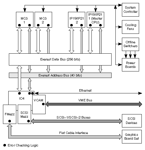
When the hardware detects an error, IRIX and the diagnostics display it in a format called the HARDWARE ERROR STATE display. This section provides a complete list of the HARDWARE ERROR STATE messages, arranged by board type. Each message contains a number representing the location of the error-checking logic (usually a bus-to-ASIC interface), as well as a description of the error bit.
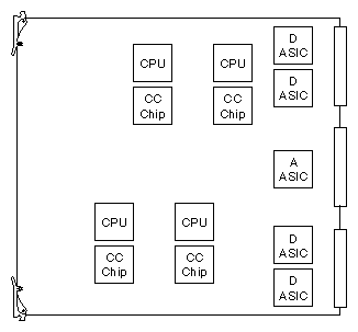
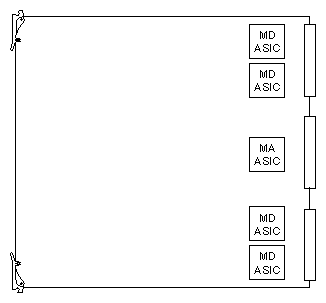
Each circuit board is represented both by a functional block diagram and by a board layout showing the physical locations of the error detection logic. Following the two figures that support each board is a table listing the possible hardware errors, along with a number that identifies where the error was detected.
Figure 2-2 is a functional block diagram of the IP19 board with the error detection points called out. Figure 2-3 shows the physical layout of the board and the locations of the error detection logic.
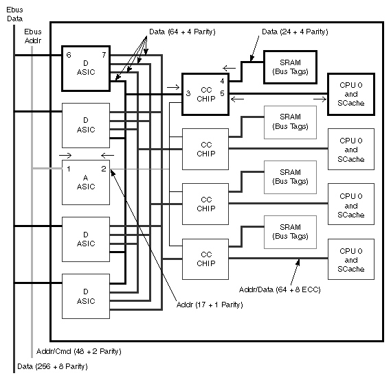
| Note: Because each of the four processor slices are identical, only the registers corresponding to slice 0 are described in the following section. |
HARDWARE ERROR STATE:
IP19 in slot 1
+      A Chip Error Register: 0xffff
+         0:CPU 0 CC->A parity error            2
+         1:CPU 1 CC->A parity error            2
+         2:CPU 2 CC->A parity error            2
+         3:CPU 3 CC->A parity error            2
+         4:ADDR_ERROR on EBUS                  1  this A chip detected that a
                                                   board emitted an address with
                                                   bad parity.
+         5:My ADDR_ERROR on EBUS               1  some board detected a parity
                                                   error in my emitted address
+
+         8:CPU 0 CC->D parity error            7  detected by D, for a cache
                                                   line write or upon an EBus
                                                   intervention reading a line
+         9:CPU 1 CC->D parity error            7
+        10:CPU 2 CC->D parity error            7
+        11:CPU 3 CC->D parity error            7
+        12:CPU 0 ADDR_HERE not asserted        1  address emitted by this A
                                                   was not decoded by any board
+        13:CPU 1 ADDR_HERE not asserted        1
+        14:CPU 2 ADDR_HERE not asserted        1
+        15:CPU 3 ADDR_HERE not asserted        1
+    CC in IP19 Slot 1, cpu 0
+    CC ERTOIP  Register: 0xffff
+        0:ECC uncorrectable error in Scache    5  detected by R4000
+        1:ECC correctable error in Scache      5  detected by R4000, upon
                                                   R4000 read or upon an EBus
                                                   intervention reading a line
+        2:Parity Error on TAG RAM Data         4  detected by CC
+        3:Parity Error on Address from A-chip  3  in path from A to CC
+        4:Parity Error on Data from D-chip     3  in path from D to CC, or
                                                   when D receives data with
                                                   bad parity from EBus.
+        5:MyRequest TimeOut on EBUS            1  A was not able to get EBus
                                                   access, to emit its request
+        6:MyResponse D-Resource TimeOut in A chip
                                                1  EBus did not return a
                                                   read-response to A
+        7:MyIntervention Response D-Resource TimeOut in A chip
                                                2  this CC returned an
                                                   intervention response to
                                                   A too late
+        8:Address Error on MyRequest on EBUS   1  one or more boards detected a                                                  parity error in A emitted
                                                   address, or ADDR_HERE not
                                                   asserted (no board decoded
                                                   A emitted address)
+        9:Data Error on MyData on EBUS         1  some board detected a parity
                                                   error in my emitted data
+        10:Internal Bus State is out of sync with A_SYNC
                                                3
+    CC in IP19 Slot 1, cpu 2
+ CC in IP19 Slot 1, cpu 3 |
| Note: The numbers following each error message correspond to the interface where the error detection logic is located. These registers are duplicated for each installed processor. |
Figure 2-4 is a functional block diagram of the IP21 board with the error detection points called out. Figure 2-5 shows the physical layout of the board and the locations of the error detection logic.
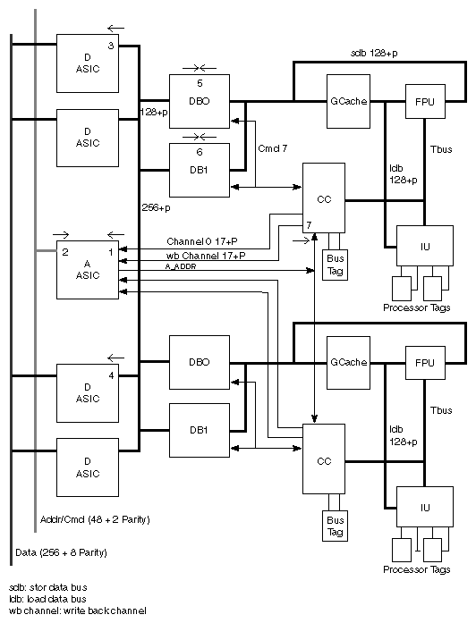
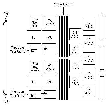
HARDWARE ERROR STATE:
IP21 in slot 1
+ A Chip Error Register: 0xffff
+ 0:CPU 0 CC->A Channel 0 parity error
+ 1
+ 1:CPU 0 CC->A Wback Channel parity error
+ 1
+ 2:CPU 1 CC->A Channel 0 parity error
+ 1
+ 3:CPU 1 CC->A Wback Channel parity error
+ 1 Error in the path between the
indicated CC Chip and the
A chip.
+ 4:ADDR_ERROR on EBUS 2 This A Chip detected an
address emitted by some
board on the EBUS with
bad parity.
+ 5:My ADDR_ERROR on EBUS 2 Some board detected a parity
error on an address emitted by
this A Chip.
+ 12:CPU 0 ADDR_HERE not asserted 2
+ 13:CPU 0 ADDR_HERE not asserted 2
+ 14:CPU 1 ADDR_HERE not asserted 2
+ 15:CPU 1 ADDR_HERE not asserted 2 A Chip emitted an address that
was not decoded by any board.
+ CC in IP21 Slot 1, cpu 0
+ CC ERTOIP Register: 0xffff
+ 0:DB chip Parity error DB0 5
+ 1:DB chip Parity error DB1 6 Need to examine other error
bits in the ERTOIP register
to determine the cause of
the problem.
If bit 7 (Data Sent
Error Channel 0) is set,
then an error occurred
between the FPU and the
DB Chip.
If bit 8 (Data Sent
Error, Wback Channel) is
set an error occurred
during the write-back of
a dirty cache line
between the Gcache and
the DB chip.
If bit 9 (Data Receive
Error) is set, it may
indicate that the data
received from the EBUS
had a parity error. It
can also indicate a
problem with one of the
D chips on the IP21
board. Look for error
indicators on other
boards to help isolate
the source of the
problem.
If none of bits 7, 8 or
9 are set, look for
error indicators on
other boards for a
possible source of the
error.
If none of bits 7, 8 or
9 are set and no errors
are indicated on other
boards, then the IP21
board introduced the
error in the path
between the EBUS and the
DB chip.
+ 2:A Chip Addr Parity 7 Indicates a parity Error
on A_ADDR[23:0], The A
chip sent something to
the CC chip containing a
parity error. Need to
interrogate other bits
to determine the cause
of the error:
If bit 5 (Address Error
on MyReq on EBus Channel
0) or bit 6 (Address
Error on MyReq on EBus
Wback channel) are
asserted in conjunction
with bit 2, the error
was introduced by the
EBus. Look for error
indicators on other
boards.
If neither bit 5 nor 6
is asserted, the error
was introduced between
the A and the CC chip
+ 3:Time Out on MyReq on EBus Channel 0
+ 4:Time Out on MyReq on EBus Wback Channel
7 Read Request sent to A
chip, never made it to
the EBUS. Indi- cates a
problem between CC and A
chip, a problem with the
A chip, or the A Chip
was prevented from
sending to the EBus by
some other board.
+ 5:Addr Error on MyReq on EBus Channel 0
+ 6:Addr Error on MyReq on EBus Wback Channel
7 If bit 2 is also
asserted (A Chip Addr
Parity), then the error
came in from the EBUS.
Look for error
indicators on other
boards to find the
source of the error.
+ 7:Data Sent Error Channel 0 5,6
+ 8:Data Sent Error Wback Channel
5,6 If this bit is asserted
without DB error (bits 0
or 1)then the error is
in the path between D
chip and DB chip.
If this bit is asserted
with DB error, then the
error is in the path
between the indicated DB
chip and the FPU.
+ 9:Data Receive Error 2 This bit is reliable
when on, unreliable when
off. Indicates that data
with an error was
received from the EBUS.
Interrogate error
indicators on other
boards to identify the
source of the error.
In particular, you may
see DB errors for other boards.
If there are no DB errors for
other boards, there may be a
problem with the IO4, memory,
or the IP21 processor itself.
+ 10:Intern Bus vs. A_SYNC10 7 The CC chip and A chip
both monitor the state
of the EBUS. This bit
set indicates that they
disagree on what state
the bus is in. Indicates
an error in the either
the CC or the A chip.
+ 11: A Chip MyResponse Data Resources Timed Out
7 Timed out on the A-chip.
Read request made it to
the bus, but never got a
response.
Note: It is possible for
the requesting CC chip
to be the cause of the
error. It may have dirty
sectors that could be
the target of the
request (for
self-intervention).
Possible problem with CC
Chip, A Chip or Bus
Tag.
+ 12:A Chip MyIntrvention Data Resources Time Out
2 Timed on the A-chip.
Read response but no
read resource allo-
cated in the A-chip.
Either an erroneous
response generated by
some other CC chip or a
failure on the A chip.
Possible problem with CC
Chip, A Chip or Bus
Tag.
+ 13:Parity Error on DB - CC shift lines
7 Local registers on the
CC chip are accessed via
the DB chip by shifting
the values in/out (CC
chip has no data path).
This bit set indicates
an error detected during
that operation. |
Figure 2-6 is a functional block diagram of the IO4 board and VCAM with the error detection points called out. Figure 2-7 shows the physical layout of the IO4 board and the locations of the error detection logic. The error messages are listed in the following section.
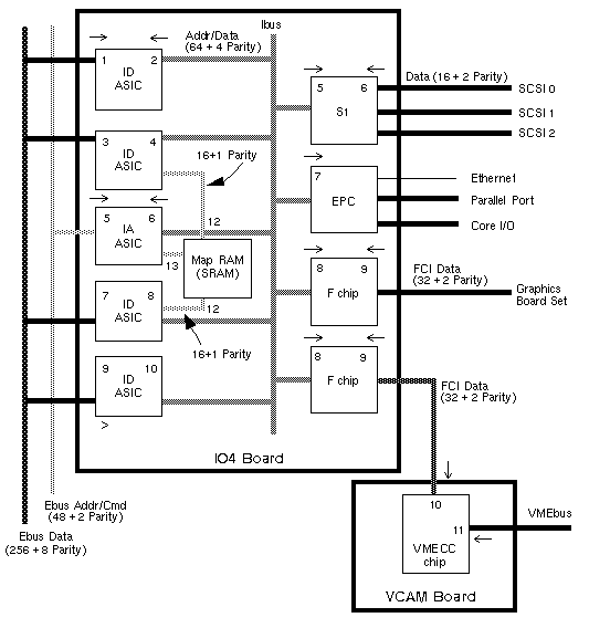
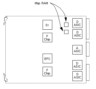
+ IO4 board in slot 5
+ IA IBUS Error Register: 0x7ffff
+ 0: Sticky Error More than one occurance of
one or more of the following
+ 1: First Level Map Error for 2-Level Mapping
12 MAPRAM data parity error
detected by ID
+ 2: 2-Level Address Map Response Command Error
4 F chip detected bad parity
on IBus operation from IA
+ 3: 1-Level Map Data Error 12 MAPRAM data parity error
detected by ID
+ 4: 1-Level Address MapResponse Command Error
4 F chip detected bad parity
on IBus operation from IA
+ 5: IA Response Data Bad On IBUS 4
+ 6: DMA Read Response Command Error 4 F chip detected bad parity
on IBus operation from IA
+ 7: GFX Write Command Error 4 F chip detected bad parity
on IBus operation from IA
+ 8: PIO Read Command Error 4 target S1/EPC/F detected
bad parity on IBus operation
from IA
+ 9: PIO Write Data Bad 4 target S1/EPC/F detected
bad parity on IBus data
from ID
+ 10: PIO write Command Error 4 target S1/EPC/F detected
bad parity on IBus operation
from IA
+ 11: PIO ReadResponse Data Error 2 ID detected bad parity
from S1/EPC/F
+ 12: DMA Write Data Error (Data From IOA)
2 ID detected bad parity
from S1/EPC/F
+ 13: DMA Write Command Error from IOA 4 IA detected bad parity
from S1/EPC/F
+ 14: PIO Read Response Command Error from IOA
4 IA detected bad parity
from S1/EPC/F
+ 15: Command Error on OP from IOA 4 IA detected bad parity
from S1/EPC/F
+ 16: IOA number of Transaction: 7 adaptor number which caused
error, only valid for errors
detected by IA or ID.
+ IA EBUS Error Register: 0xfe0003ff
+ 0: Sticky Error
+ 1: My DATA_ERROR Received 3 one or more boards detected
a parity error in my emitted
data, emitted by ID
+ 2: ADDR_ERROR Detected 3 this IA detected either
another board emitted an
address with bad parity, or
ADDR_HERE not asserted (no
board decoded someones
emitted address)
+ 3: Non Existent IOA 3 No F/S1/EPC configured at
specified address, probable
software error
+ 4: Illegal PIO 3 CC Write Gatherer block
write only allowed to F+FCG,
probable software error
+ 5: My ADDR_ERROR Received 3 one or more boards detected a parity error in IA emitted
address, or ADDR_HERE not
asserted (no board decoded
IA emitted address)
+ 6: EBUS_TIMEOUT Received 3 IA was not able to get
EBus access, to emit its
request
+ 7: Invalidate Dirty Exclusive Cache Line
3 EBus cache coherence
protocol violation detected
by IA
+ 8: Read Resource Time Out 3 EBus did not return a
read-response to IA
+ 9: DATA_ERROR Received 3 ID detected bad parity
on data from EBus
+ 25: PIO Queue full for Adapter 1 4 S1/EPC/F is not responding
+ 26: PIO Queue full for Adapter 2 "
+ 27: PIO Queue full for Adapter 3 "
+ 28: PIO Queue full for Adapter 4 "
+ 29: PIO Queue full for Adapter 5 "
+ 30: PIO Queue full for Adapter 6 "
+ 31: PIO Queue full for Adapter 7 "
+ IA Error Ebus Address: 0x4 Holds the EBus address of
the transaction which caused
a parity error on EBus.
Valid if bit 5 in this
register is set.
+ 40: EBus Outgoing Command: 0x54 Command on EBus which caused
parity error on EBus
+ EPC in IO4 slot 5 adapter 1
+ Ibus Error Register: 0x3e6311
+ 3..0: EPC Detected- PIO Write Request Data Error from IA
7
+ 3..0: EPC Detected- DMA Read Response Data Error from IA
7
+ 3..0: EPC Detected- Unexpected DMA Read Response Error from IA
7
+ 3..0: EPC Detected- Undetermined Command Error from IA
7
+ 11..4: EPC Observed- PIO Write Request Data Error from IA to IOA 3
7
+ 11..4: EPC Observed- GFX Write Request Data Error from IA to IOA 3
7
+ 11..4: EPC Observed- DMA Read Response Data Error from IA to IOA 3
7
+ 15..12: EPC Sent- PIO (to EPC) Read Response Command Error to IA
7 Error from EPC to IA
+ 15..12: EPC Sent- PIO (to EPC) Read Response Data Error to IA
7 Error from EPC to IA
+ 15..12: EPC Sent- DMA (Enet) Read Request Command Error to IA
7 Error from EPC to IA
+ 15..12: EPC Sent- DMA (Enet) Write Request Command Error to IA
7 Error from EPC to IA
+ 15..12: EPC Sent- DMA (Enet) Write Request Data Error to IA
7 Error from EPC to IA
+ 15..12: EPC Sent- Interrupt Request Command Error to IA
7 Error from EPC to IA
+ 15..12: EPC Sent- PIO (thru EPC) Read Response Command Error to IA
7 Error from EPC to IA
+ 15..12: EPC Sent- PIO (thru EPC) Read Response Data Error to IA
7 Error from EPC to IA
+ 15..12: EPC Sent- DMA (PPort) Read Request Command Error to IA
7 Error from EPC to IA
+ 15..12: EPC Sent- DMA (Pport) Write Request Command Error to IA
7 Error from EPC to IA
+ 15..12: EPC Sent- DMA (Pport) Write Request Data Error to IA
7 Error from EPC to IA
+ 16: Parity Error on IBusAD[15:0]
+ 17: Parity Error on IBusAD[31:16] 7 Error from EPC to IA
+ 18: Parity Error on IBusAD[47:32] 7 Error from EPC to IA
+ 19: Parity Error on IBusAD[63:48] 7 Error from EPC to IA
+ 20: Error Overrun
+ 21: DMA Read Response 1 msec Timeout Error
+ IBus Opcode+Address: 0x2a40 7 Holds the IBus contents if
EPC detects an error in IA
initiated transaction
+ Fchip in IO4 slot 5 adapter 3, FCI master: FCG
F chip connects
to graphics
+ Fchip in IO4 slot 5 adapter 2, FCI master: VMECC
F chip connects
to VME bus
+ Error Status Register: 0x4ffffff
+ 0: OverWrite
+ 1: Loopback Received
+ 2: Loopback Error
+ 3: F to IBus Command Error - non-interruptable
8 IA detected parity error
on command from F
+ 4: PIO Read Response IBus Data Error - non-interruptable
8 ID detected parity error
on data from F
+ 5: DMA Read Request Timeout Error 8 IA did not return DMA
read response
+ 6: Unknown IBus Command Error 8 F detected parity error
on command from IA
+ 7: DMA Read Response Ibus Data Error 8 F detected parity error
on data from ID
+ 8: DMA Write Data FCI Error 9 F detected parity error
on data from FCI
+ 9: PIO Read Response FCI Data Error 9 F detected parity error
on data from FCI
+ 10: PIO/GFX Write IBus Data Error 8 F detected parity error
on data from ID
+ 11: Load Address Read FCI Error 9 F detected parity error
on address from FCI
+ 12: DMA Write IBus Command Error 8 IA detected parity error
on command from F
+ 13: Address Map Request IBus Command Error
8 IA detected parity error
on command from F
+ 14: Interrupt IBus Command Error 8 IA detected parity error
on command from F
+ 15: Load Address Write FCI Error 9 F detected parity error
on data from FCI
+ 16: Unknown FCI Command Error 9 F detected parity error
on command from FCI
+ 17: Address Map Request Timeout Error 8 IA did not return map
response
+ 18: Address Map Response Data Error 8 F detected parity error
on data from ID
+ 19: PIO F Internal Write IBus Data Error
8 F internal problem
+ 20: IBus Surprise 8 F received unexpected
bus-grant/DMA-response
from IA
+ 21: DMA Write IBus Data Error 8 ID detected parity error
on data from F
+ 22: System FCI Reset
+ 23: Software FCI Reset
+ 24: Master Reset 9 F received a reset request
from FCI
+ 25: F Error FCI Reset 9 F reset FCI due to some error
+ 26: F Chip Reset in Progress
+ 27: Drop PIO Write Mode 8 F unrecoverable error
+ 28: Drop DMA Write Mode 8 F unrecoverable error
+ 29: Fake DMA Read Mode 8 F unrecoverable error
+ IBus Opcode+Address: 0xa54b 8 captures the F operation
which received a parity
error.
+ FCI Error Command: 0x3f 9 captures the FCI command
which had a data parity error
+ VMECC in IO4 slot 5 adapter 2
+ Error Cause Register: 0x1fff
+ 0: VME Bus Error on PIO Write (interrupts)
11 error from VME
+ 1: VME Bus Error on PIO Read (no interrupt), return bad parity data
11 error from VME
+ 2: VME Slave Got Parity Error (no interrupt)
10 detected error on FCI
+ 3: VME Acquisition Timeout by PIO Master (interrupt, set dropmode)
11 error from VME
+ 4: FCIDB Timeout (no interrupt) 10 detected error on FCI
+ 5: FCI PIO Parity Error (interrupt) 10 detected error on FCI
+ 6: Overrun among bit 0,1,3,4,5
+ 7: in Dropmode
+ VME Address Error Register: 0xa0001248
+ Extra VME Bus signal register: 0x19e49
+ AM: 0x9 IACK Read AS DS0 DS1
+ VME-Grant-Level: 1: VME backplane levels
+ S1 in IO4 slot 5 adapter 4
+ S1 Command Status Register: 0xffff
+ 6 : Error in SCSI Data DMA channel 0 6 detected error from SCSI
+ 7 : Error in SCSI Data DMA channel 1 6 detected error from SCSI
+ 8 : Error in SCSI Data DMA channel 2 6 detected error from SCSI
+ 9 : PIO Read Error in SCSI 0 6 detected error from SCSI
+ 10: PIO Read Error in SCSI 1 6 detected error from SCSI
+ 11: PIO Read Error in SCSI 2 6 detected error from SCSI
+ 12: PIO Write data Overrun due to PIO FIFO Full
5 S1 internal error
+ 13: Missing Write data during PIO write
5 S1 detected error on IBus
+ 14: PIO with an invalid address 5 S1 detected error on IBus
+ 15: PIO Drop mode active 5 S1 detected error on IBus
+ S1 Ibus error Register: 0x1fffffff
+ 1: Error on Incoming Data to S1 - multiple occurances
5 S1 detected error on IBus
+ 2: Error on Incoming command to S1 - multiple occurances
5 S1 detected error on IBus
+ 3: Error on Outgoing data from S1 - multiple occurances
5 S1 detected error on IBus
+ 4: Error on Outgoing command from S1 - multiple occurances
5 S1 detected error on IBus
+ 5: Error in DMA translation - multiple occurances
5 S1 detected error on IBus
+ 6: Error in Channel 0 - multiple occurances
+ 7: Error in Channel 1 - multiple occurances
+ 8: Error in Channel 2 - multiple occurances
+ 9: Surprising DMA Read/Ibus Grant - multiple occurances
5 S1 detected error on IBus
+ 10: PIO Read response Error - multiple occurances
5 IA detected error in data
from S1
+ 11: PIO Write request Error - multiple occurances
5 S1 detected error on IBus
+ 12: DMA Read response Error - multiple occurances
5 S1 detected error on IBus
+ 13: Interrupt Error - multiple occurances
5 IA detected error
+ IBus Opcode+Address: 0xbfe0 5 holds the S1 emitted IBus
operation where a Parity
error was reported by IA |
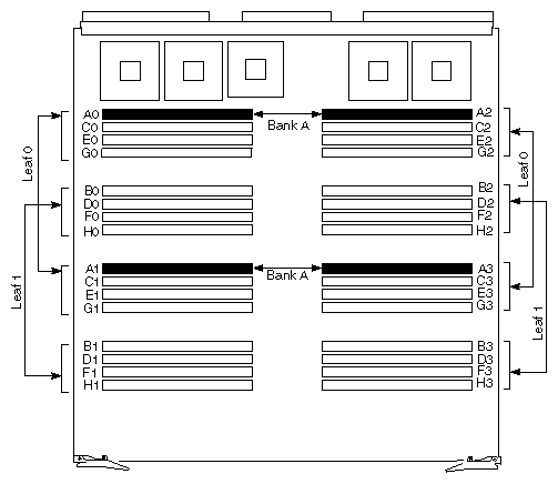
Figure 2-8 is a functional block diagram of the MC3 board showing the error detection. Figure 2-9 shows the physical layout of the board and the locations of the error detection logic. The error messages are listed in the following section.
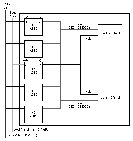
+  MC3 in slot 3
+      MA Ebus Error register: 0xf
+        My EBus Address Error                  3 destination board detected
                                                  a parity error in MA emitted
                                                  read-response ? field
+        My EBus Data Error                     3 one or more boards detected
                                                  a parity error in MD emitted
                                                  read-response data
+        EBus Address Error                     3 this MA detected another
                                                  board emitted an address with
                                                  bad parity
+        EBus Data Error                        1 this MD received data with
                                                  bad parity
+      MA Leaf 0 Error Status Register: 0xf
+        Multiple Occurence of these errors:      Shows more than one Read
                                                  Single Bit Error occurred
+        Read Single Bit Error                  2 correctable error in this
                                                  leaf
+        Read Uncorrectable Error               2 uncorrectable error in this
                                                  leaf
+        PartialWrite Uncorrectable Error       2 uncorrectable error upon
                                                  reading out this leaf, to do
                                                  a partial write merge
+ MA Leaf 1 Error Status Register: 0xf |
This section groups various troubleshooting/debugging tips. Some of the methods described require equipment that is not readily available in the field, and are better suited for use by manufacturing or a repair depot.
This section describes common CPU board problems and their solutions.
| Note: Before starting to troubleshoot the board, verify that both the 3.3V and 5.0V bricks are working within acceptable levels. If the 5.0V brick fails while the 3.3V brick continues to work, the ASICs will overheat. |
Check the power fault LEDs on the board (see Figure 2-3).
If the fault LEDs are off, but the bricks are still suspect, check the voltages at the red and black test points at the back of the board.
| Note: If the 5.0V brick has failed, it will still show approximately 2.5V, owing to the 3.3V brick pulling up through the ASICs. |
There is a power or ground short.
The LED controller PAL has failed.
One or more of the R4KIO PALs has failed. Check the PALs on the failing slices. The PALs are at locations I5H1, J1M0, I3J9, and F2E1 for slices 0 through 3, respectively.
The processors are not booting from their EAROMs and PROMs.
Check for missing clocks.
Check for bad PROMs or PALs.
Check for a dead processor.
The clocks may not be running. Check the clocks as follows:
Look for a 50-MHz ECL-level clock at pin F8.
Check the MC100E11 backplane clock driver at G0C8.
Check that the MC100E11 power supply is at 4.5V.
Look for a 50 or 75-MHz TTL-level clock at pin V4.
If no clock is present, check the local crystal at G9K7 or H5K7.
Check the driver at G9J8. Clock pulses should be present at pins 12, 14, 16 and 18.
Look for a clock at pin V4 of the failing slice's CC chip.
If no clock is present, check the R4k Reset PAL. The PALs are located at F9G5, G1K7, I3J9, and I7G5 for processor slices 0 through 3, respectively.
Note: If the clock is running at 25 percent frequency, the EAROM is probably faulty. Check that the processor is securely seated in the socket. Remove the heat sink and check for snugness.
Check the R4kIO PAL, EAROM, and processor, as noted previously.
Replace the EPROM and check the board again.
Check the frequency of the ModeClk at N19. The frequency should be approximately 200 kHz. If no ModeClk signal is present, the processor has failed.
Check the reset line (pin 20) to the CC chip.
If the reset line does not pulse when the SCLR line is enabled, check pin 17 on the A chip.
If the A chip line doesn't pulse either, check for a failure in the System Controller.
This procedure assumes that the processor is basically functional. It can fetch and execute EPROM instructions, but may be having trouble reaching the bus or ASICs beyond the CC chip.
Record the binary LED value and refer to Section 5.7, "CPU Board Fault/Status Indicators," for a description of the fault.
Check the UART output.
From a working board in the same system, read register 0 on the board under test. This is done by using the POD command dc <slot number> 0. Register 0 contains the ENABLE vector, which represents the number of processors populating the board.
For the IP19, the value 0x3 corresponds to two CPUs and 0xf corresponds to four CPUs. For the IP21, the value 0x3 corresponds to one CPU and 0xf corresponds to two CPUs.
If the register value does not match the number of occupied slices, replace the CC_SHARED PAL at G0C0.
The serial clock is not running.
Look for approximately 100 kHz at pin 20 on the CC chip.
If no clock is present, check the System Controller for serial clock generation.
The serial clock is not running. Diagnose per Section 2.5.1.9, "IP19 LEDs Show a Static 0xe Pattern."
System is stuck in bootmaster arbitration. Possible cause is a CC clock problem.
Replace the CC chip.
Replace the EAROM.
System is stuck in bootmaster arbitration. Diagnose per Section 2.5.1.11, "IP19 LEDs Show a Static 0xc Pattern."
Check UART cable and connections.
Verify that the serial clock is matched to the UART speed. When connecting to the UART, match the speed with the System Controller speed.
| Note: The standard System Controller produces a 9600 baud clock. |
If an IO4 failure occurs during the boot process, the error message will continue to scroll across the System Controller display until the system is powered off. Clear the display by first turning the key switch to the Manager position. Enter the Debug Settings menu and set the Manu-Mode bit. Setting this bit sends the IP19 and IP21 PROM error messages to the external UART on the System Controller (see Section 2.5.3, "Using the System Controller").
This section contains various troubleshooting procedures using the System Controller.
This section shows how to connect an ASCII terminal to a system with a faulty IO4 board, bad monitor, or bad terminal.
The workaround is based on the System Controller's connection to all of the CC chips on the lowest-numbered CPU board, over the polled serial bus. The polled serial bus is composed of six address lines and two data lines, and is used primarily during the bootmaster arbitration process. The System Controller can address all of the processors through their respective CC chips, but only the bootmaster CPU is capable of responding.
A port (or UART) is tied directly to the System Controller. You can attach a terminal to this port and use it to reach the CPU board by going through the controller and over the polled serial bus. On rack-mounted systems, the System Controller UART is located in the lower left corner of the midplane (when facing the front of the chassis). Deskside systems have the UART located in the lower right corner of the backplane (when facing the rear of the chassis). The port is labeled External Controller Serial on all systems.
| Note: The System Controller UART is equipped with a permanently attached cable with a DB-25 connector at the terminal end. |
Select the Debug Settings menu and toggle bit 7 (the Manu-Mode bit) to select the System Controller UART. Refer to Section 4.5.2, "Key Switch in the Manager Position" for more information on the Debug Settings menu.
TTT provides some commands you can use over the System Controller port.
Table 2-2. System Controller Commands
Task | Command | Comment |
|---|---|---|
Get processor out of slave mode | <Ctrl>-xsuz<Ctrl>-y | Pressing <Ctrl>-x s begins the select command, u indicates the CPU slot number, z specifies the slice number, and <Ctrl>-y executes the command. No spaces between keystrokes; do not press <Enter>. |
Select processor to communicate with | selectx | x is the processor slice. The new
prompt will take the form |
Put all selected processors in a slot into POD mode | <Ctrl>-p | All processors selected with the select command are placed in POD mode. |
Exit POD mode | reset | Returns you to the PROM Monitor. |
Cycle system power | <Ctrl>-xc<Ctrl>-y | No spaces between keystrokes; do not press <Enter>. |
Reset the system | <Ctrl>-xr<Ctrl>-y | No spaces between keystrokes; do not press <Enter>. |
Force a non-maskable interrupt (NMI) | <Ctrl>-xn<Ctrl>-y | No spaces between keystrokes; do not press <Enter>. |
Defeat the System Controller when you suspect a dead controller or bad sensor.
Cycling the key switch while pressing the Execute button allows the System Controller to come up without starting the power-on sequence. This is valuable if an error such as a power fault generates a repeating message on the display. The error log can then be checked and the voltage protection turned off using the Debug Settings menu (refer to Section 4.5.2, "Key Switch in the Manager Position").
Return to the default debug settings by simultaneously pressing the Menu and Scroll Down buttons while cycling the key switch.
Cycle the key switch to return to normal controller operation.
When a processor fails, it is disabled by the system. Because a disabled processor is unable to talk to the system bus, you cannot use IDE to diagnose the cause of the fault. Enable the processor by first turning the key switch to the Manager position. Select the Debug Settings menu and set the No Diagnostics bit. Power cycle the system to activate the change to the debug settings menu and enable the faulty processor. See Section 4.5.2, "Key Switch in the Manager Position," for additional information on the Debug Settings menu.
The following describes how to make and use a debug kernel to help diagnose system hangs. With a debug kernel, the debugger symmon boots along with the kernel when the system is started.
Follow these steps to create and boot a debug kernel:
Set the system console to the serial port using the PROM monitor.
In /var/sysgen/system/irix.sm, find the line with idbg. Change EXCLUDE to INCLUDE.
Go to the end of the file and remove the asterisk (*)from the CCOPTS line containing -XNp, and add an asterisk (*) to the other CCOPTS line
Remove the asterisk (*) from the LDOPTS line containing -T 80100000, and add an asterisk (*) to the other LDOPTS line. Note that CCOPTS and LDOPTS lines are paired. This causes the kernel to be shifted in memory to make room for the debugger.
Run the command autoconfig from the command line.
Boot this kernel. It should automatically bring in symmon.
Allow the machine to hang; induce it if the hang is repeatable, or run the system until the hang occurs. When a hang occurs, follow these steps to use the debug kernel:
When the hang occurs, press <Ctrl>-A on the serial console. You should see the following prompt:
DBG:
If there is no response when you press <Ctrl>-A on the system console, use the front panel of the System Controller to issue a nonmaskable interrupt (NMI).
If there is a DBG: prompt on the console, press <Ctrl>-A again and continue with the next step.
If issuing an NMI does not place the system in debug mode (no DBG: prompt is displayed), you cannot continue. Issue a second NMI to place the system in POD mode, from which you can use further diagnostics as described in Chapter 5, "PROM Monitor."
Enter the following command at the DBG prompt:
stop
Next, enter the cpu command to display a list of processors:
cpu
You should see a list of stopped processors. Normally, all of the CPUs in the system should be listed. A hardware hang problem often shows up as a processor missing from this list. If this is the case, suspect a problem with the CPU.
IP19 only: If a CPU is missing from the hardware list and the IP19 board is not at revision -007 or later, it is especially likely a CPU problem.
If all the CPUs are listed, enter the following commands at the DBG prompt:
hwstatepb
The pb command displays the last few kernel messages from the putbuffer. Look for any messages that indicate a stack underflow or stack overflow. These suggest a software problem rather than a hardware problem. Also, enter this command:
ubt
Reporting the results of the ubt command can help find the cause of stack overflows.
If the ubt stack backtrace shows the function trap(0xffffxxxx, ...), enter the efr command using the first argument to trap:
efr 0xffffxxxx
Use this procedure when the system does not respond to a single NMI.
At the System Controller front panel, turn the key switch to the On position.
Press and hold the two center buttons and simultaneously turn the keyswitch to the Manager position (full clockwise).
Release the two center buttons.
Press the Menu button, and scroll to the Debug Settings menu entry (which does not appear until the preceding steps are performed).
Press the Execute button.
At this point, sixteen debug switch bits are displayed. The bit number of the cursor is at the right side of the screen. Use the two center buttons to move the cursor to bit 4, then use Execute to toggle it to 1. Move the cursor to bit 5 and use Execute to toggle it to 1.
Press the Menu button to finish. The Debug Settings option disappears.
Reset the system from the front panel. The system should automatically enter POD mode and you should see the POD mode prompt:
pod >>
When you are finished using POD mode, repeat steps 1 through 7, and reset bits 4 and 5 so that the system boots normally.
The following procedure, run from POD mode, can determine if an MC3 board has a clock jitter problem:
Enter POD mode. To enter POD mode, use the procedures outlined in Section 4.5.2, "Key Switch in the Manager Position" or Section 2.5.5, "Procedure to Cause a Hung System to Enter POD Mode."
At the POD prompt, enter the command info to display boards in slots. Note which slots contain MC3 boards.
Enter the command dmc dd, where dd is the hex slot number of an MC3. Do this for each slot containing an MC3 board. See Section 5.6.4, "Using POD to Examine HARDWARE ERROR STATE Messages" for complete information on interpreting the output of the dmc command.
Examine the EBus Error and Error = fields for:
EBus Error, bits 2 or 3 set (0x4 or 0x8)
and
Leaf 0 and Leaf 1 "Error =" field is 0
These messages indicate an MC3 problem, most likely clock jitter. To fix this requires upgrading the MC3 or trying the voltage reduction workaround described in the Challenge/Onyx Retrofit II Requirements document.
If the Leaf 0 or Leaf 1 Error = field has any bits set, there is an MC3 SIMM problem.
Everest hardware errors are displayed following IRIX kernel panics, in the IDE stand-alone diagnostics, and in some of the PROM-based power-on tests. The display format of the error messages is referred to as the HARDWARE ERROR STATE, and is defined as follows:
The only bits displayed are those indicating an error has been detected. Normal bits are not displayed.
The display walks through all the boards in the system and through every ASIC on each board.
A HARDWARE ERROR STATE display consists of the banner line HARDWARE ERROR STATE: followed by indented lines prefixed by a plus (+) sign. Line indentation, from left to right, indicates the board, the ASIC, the register, and the bit. For example:.
HARDWARE STATE:
+IP19 in slot 1 (CPU Board)
+CC in IP19 slot 1, CPU 0 (ASIC on CPU Board)
+CC ERTOIP Register: 0xffff (Register in the CC and its hex value)
+Parity Error on TAG RAM Data (Bit in the register that is set)
Each error register's value is shown in hexadecimal, followed by a line for each bit set.
Each board identifies its location with its board slot number. Each ASIC identifies its location with some address information: a CC by the CPU it is associated with, the EPC, F chip, or S chip by its Ibus adapter number.
| Note: The F chip also identifies the ASIC that is at the other end of its flat cable. |
The decimal bit number precedes the name of each error bit.
Some registers have multibit values and are displayed in hexadecimal rather than as bits.
The kernel will panic in response to many possible hardware errors. The HARDWARE ERROR STATE messages allow you to trace the error back to the ASIC that originally detected the fault, thereby identifying the FRU to be replaced. Relate the error message to a block diagram of the system, and walk the propagated errors backwards to determine where the fault originated.
As an example, assume that a driver, executing on an IP19 CPU, attempts to read a control register on a VMEbus device. If the controller fails to respond, the VMEbus will time-out. The time-out causes the VMECC to record VME Bus Error on PIO Read. The VMECC will return an error message to the F ASIC. From the F ASIC, the error passes through the IA ASIC, the A ASIC, and the CC chip and finally reaches the CPU as a bus error. Each of the ASICs in this sequence may record the error. The kernel panics and dumps all of the set error register bits. You must understand the possible error propagation paths throughout the machine to distinguish the secondary, propagated errors from the origin of the fault.
This section lists some known hardware and software problems, as of this writing.
Bugs in IRIX 5.0.1 can cause software hangs. Try to move the customer to the latest release of the IRIX operating system.
If the customer is not using paging and file quotas, make sure the customer's system is running IRIX 5.2 (plus patch 0 and patch 22) or later.
A likely cause of hangs is the MC3 board clock jitter problem. Diagnose it by examining the HARDWARE ERROR STATE of the MC3. Section 2.5.5 shows how to identify it, with the pod dmc command.
MC3 clock jitter is usually indicated by the following error message:
WARNING: (Kernel) Bus Error Exception ... HARDWARE ERROR STATE + MC3 in slot s + MA EBus Error register: 0x4 + 2: My EBus Data Error + IP19 in slot s + CC in IP19 slot s, cpu c + CC ERTOPI Register: 0x10 + 4:Parity Error on Data from D-chip |
The part of this message that pinpoints the MC3 is My EBus Data Error. However, if you also see this message, it may not be an MC3 clock jitter problem:
+ MA Leaf 0 Error Status Register: 0x2 + 1: Read Uncorrectable (Multiple Bit) Error |
If you see the Read Uncorrectable message, it is more likely a SIMM problem.
| Note: Do not consider only one part of the message in isolation; for example, when looking for the message My EBus Data Error, you must also look for the presence or absence of additional error bits. This is because when an IP19 or IP21 D chip detects a parity error incoming from the EBus, it both records bit 4 and sends a signal back to the sender. It is at that point that the MC3 that issued the EBus cycle issues the message My EBus Data Error. |
This problem also shows up as a system hang, where the system does not echo characters on the serial console, not respond to network pings, and there is no disk or power meter activity. The procedure in Section 2.5.5 can also help to pinpoint the bad MC3.
To deal with the clock jitter problem, there is an MC3 board with a KL-1 daughter card. When this board is not available, there is a valuable workaround, which eliminates the problem in many MC3 boards, called the "MC3 voltage reduction workaround." The workaround is described in the Challenge/Onyx Retrofit II Requirements document.
Sometimes the MC3 does not properly record errors. When an uncorrectable memory error is detected during certain phases of data transfer, the MC3 may fail to record the error, or incorrectly signal the error on a subsequent bus cycle.
Even if the error is not recorded, the MC3 still sends the data with bad parity. The CPU board then records a Parity Error on data from d-chip. This is believed to the single most frequent cause of an IP19 signaling the following message (with no other bits set):
+ IP19 in slot 3 + CC in IP19 Slot 3, cpu 1 + CC ERTOIP Register: 0x10 + 4:Parity Error on Data from D-chip |
The above symptom is probably caused by a failing MC3 or SIMM.
This problem appears similar to MC3 clock jitter. If a single bit error is encountered on the ECC check bits, the MC3 will incorrectly signal a parity error on the EBUS. It may or may not indicate My EBus Data Error, depending on the conditions listed in Section 2.7.4, "MC3 Error Latching."
+ MC3 in slot s + MA EBus Error register: 0x4 + 2: My EBus Data Error + IP19 in slot s + CC in IP19 slot s, cpu c + CC ERTOPI Register: 0x10 + 4:Parity Error on Data from D-chip |
This problem is also indicative of a failing MC3 (or SIMMs).
Uncommonly high error rates have been seen with type III SIMMs. A new test is now used to catch marginal or failing SIMMs in manufacturing. If ECC errors or system hangs are being seen in a system whose MC3 boards have been replaced, or are otherwise up to date, the SIMMs should be replaced.
There is an EAROM for each CPU on an IP19 board. A board problem, in IP19 boards earlier than -008 (-008 is fixed), could occasionally alter the EAROM at power-on. The fixed board also contains an EAROM updated with a checksum.
With IRIX 5.1 or later, the IO4 PROM Version 1.09 automatically corrects common cases of corruption. It also displays a checksum of all EAROMs, in this message:
Starting processor #1 Starting processor #2 ... Comparing EAROM checksums... EAROM checksums: 092e 092e 092e ... Checking hardware inventory... |
The checksum values are 16 bit hex in the processor numbering sequence. With the fixed IP19 board, where the EAROM contains a checksum, no value is displayed (it is just verified).
To confirm that a system has good EAROMs, record the PROM boot messages and compare them against this table:
R4400 100MHz, 1M Scache: 092e R4400 150MHz, 1M Scache: 086b R4400 100MHz, 4M Scache: 0930 R4400 150MHz, 4M Scache: 086d |
If the IO4 PROM Version 1.09 or later does not display the message Comparing EAROM checksums, then the EAROMs have tested as good.
This problem produces the same message sequence as MC3 clock jitter. With a sudden burst of Ebus traffic, a power supply can take up to 3 milliseconds to supply enough current. In this period, a backplane termination voltage can droop, reducing noise the margin, or possibly triggering the System Controller low-voltage detector.
This voltage droop results in either
an Ebus parity error, or
a POKB error (causing an immediate system power-off).
An Ebus parity error shows up in the HARDWARE ERROR STATE messages as
Parity Error on Data from D-chip |
along with an MC3 board showing the following message:
My EBus Data Error |
The POKB error is displayed on the System Controller front panel.
If you suspect this, check the termination voltage supplied by the System Controller. Use the Voltage Status menu on the front panel. It should read 1.6 volts. If it does not, it is likely that backplane voltage droop is causing the errors.
You can also use the sysctrlrd command to examine the voltages. Log in as root and enter the following command from the shell prompt:
/usr/etc/sysctlrd -p |
To resolve this problem and ensure reliable system operation, apply deviation DA798 to increase the termination voltage for the System Controller. This deviation raises the termination voltage from 1.5 volts to 1.6 volts.
The following message is a sign of possible MC3 SIMM failure:
HARDWARE ERROR STATE: + MC3 in slot 1 + MA EBus Error register: 0x4 + 2: My EBus Data Error + MA Leaf 1 Error Status Register: 0x2 + 1: Read Uncorrectable (Multiple Bit) Error + MA Leaf 1 Bad Memory Address: 0x1df47b80 + IP19 in slot 2 + CC in IP19 Slot 2, cpu 3 + CC ERTOIP Register: 0x10 + 4:Parity Error on Data from D-chip |
The MC3 is showing Read Uncorrectable (Multiple Bit) Error, meaning the MC3 had an ECC error in its SIMM and therefore purposely encoded a response to the IP19 with parity error set. Therefore, the IP19 error message Parity Error on Data from D-chip is a result of the MC3 ECC problem and so is the MC3 My EBus Data Error. The ECC in the MC3 SIMM is the problem.
Occasionally there is a VME bus error on a PIO read. It occurs when a driver performs a PIO read on a VME device that does not respond. The VME bus times out, and the following error message is displayed:
pb 0: + IP19 in slot 3 pb 1: + CC in IP19 Slot 3, cpu 1 pb 2: + CC ERTOIP Register: 0x10 pb 3: + 4:Parity Error on Data from D-chip pb 4: + IO4 board in slot 11 pb 5: + IA IBUS Error Register: 0x30800 pb 6: + 11: PIO ReadResponse Data Error pb 7: + 18..16: IOA number of Transaction: 3 (VMECC) pb 8: + IA EBUS Error Register: 0x2 pb 9: + 1: My DATA_ERROR Received pb 13: + Fchip in IO4 slot 11 adapter 3, FCI master: VMECC pb 14: + Error Status Register: 0x201 pb 15: + 0: OverWrite pb 16: + 9: PIO Read Response FCI Data Error pb 17: + VMECC in IO4 slot 11 adapter 3 pb 18: + Error Cause Register: 0x2 pb 19: + 1: VME Bus Error on PIO Read (no interrupt), return bad parity data pb 20: + VME Address Error Register: 0x480bbe5c pb 21: + Extra VME Bus signal register: 0x1df pb 22: <0>PANIC: CPU 1: Bus Error Exception in User mode ... |