This Chapter describes the power-on tests, describes how the Everest boards are configured, and explains the Monitor boot commands.
The power-on tests are initiated when the System Controller sends the SCLR signal, resetting the processors. This series of tests begins with the CPU logic supporting each individual processor and expands to test and configure the entire system. Although the sequences for the IP19 and IP21 are similar, there are differences in the order and type of power-on tests.
Section 5.2.1 describes the IP19 power-on tests, and Section 5.2.2 describes the IP21 power-on tests.
The power-on test sequence for the IP19 CPU board is illustrated in the flowchart that spans Figure 5-1 through Figure 5-4.
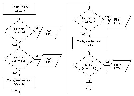
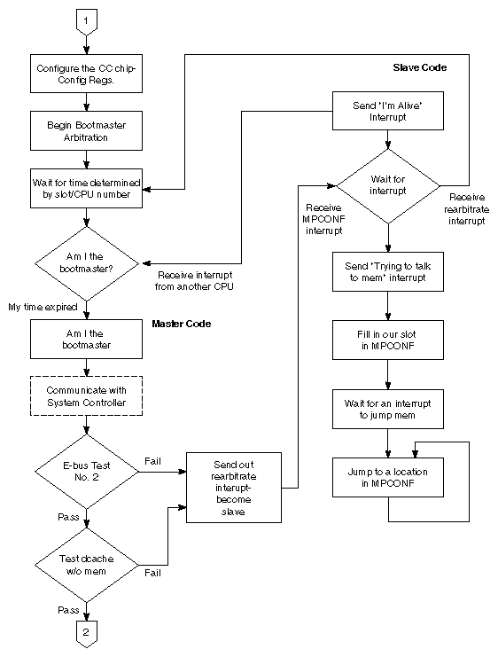
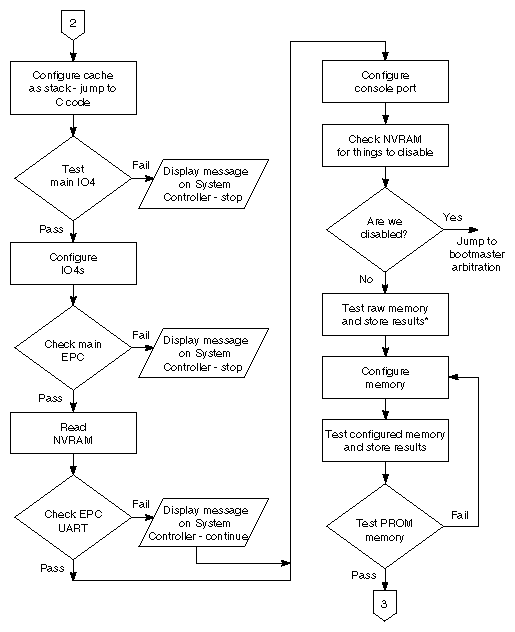
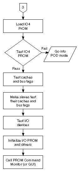
The power-on test sequence for the IP19 CPU board is illustrated in the flowchart that spans Figure 5-5 through Figure 5-8
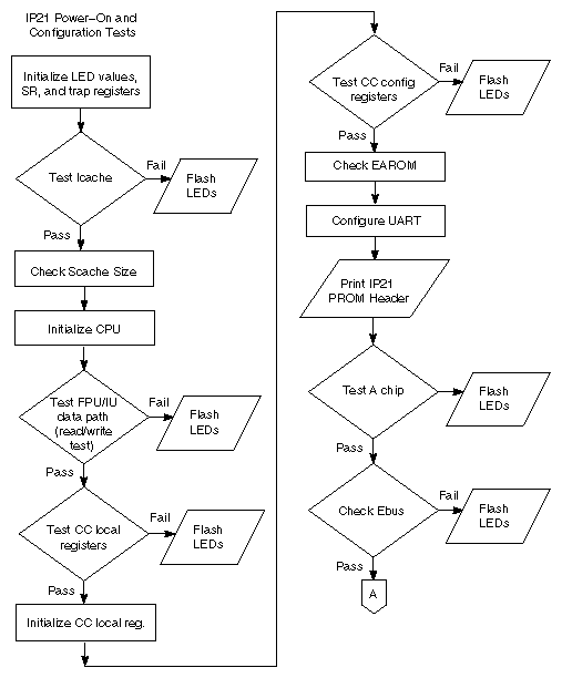
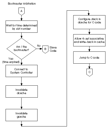
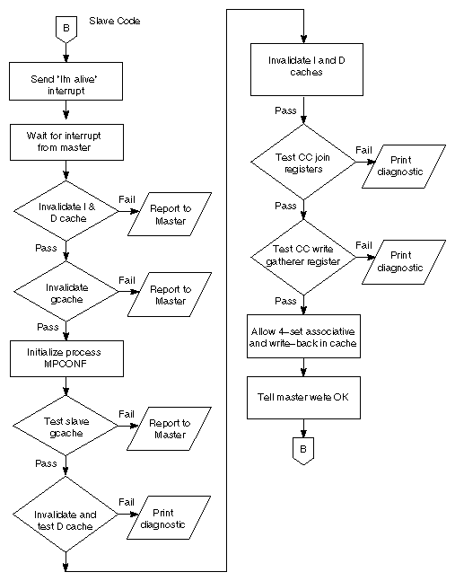
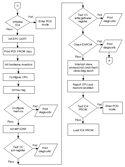
This section lists of all of the status messages that are displayed by the System Controller during the normal power-on process for IP19-based systems. IP21 systems vary slightly. The messages are listed in the order in which they appear.
Starting System...
Displayed once bootmaster arbitration has completed. Indicates that the master processor has started up correctly and is capable of communicating with the system controller.EBUS diags 2...
Displayed immediately before we run the secondary EBUS diagnostics. The secondary EBUS diagnostics stress the interrupt logic and the EBUS.PD Cache test...
Displayed immediately before we run the primary data cache test.Building stack...
Displayed before we attempt to set up the cache as the stack. If this is the last message displayed, there is probably something wrong with the master processor.Jumping to MAIN...
Displayed before we switch into the C main subroutine.Initing Config Info...
Displayed before we attempt to do initial hardware probing and set up the everest configuration information data structure. In this phase, we simply read out the SYSCONFIG register and set the evconfig fields to rational default values.Setting timeouts...
Displayed before we attempt to write to the various board timeout registers. Everest requires that all of the boards be initialized with consistent timeout values, and that these timeout values be written before we actually do reads or writes to the boards (we're safe so far because we have only touched configuration registers; this will change when we start talking to IO4 devices).Initing master IO4...
Displayed before we attempt to do basic initialization for all of the IO4's in the system. Basic initialization consists of writing the large and small window registers, setting the endianess, setting up error interrupts, clearing the Ibus and Ebus error registers, and examining the IO adapters.Initing EPC...
Displayed before we do the first writes to the master EPC. This routine clears the EPC error registers and takes all EPC devices out of reset.Initing EPC UART...
Displayed when we first enter the UART configuration code.Initing UART Chan B...
Displayed before we begin initializing UART channel B's control registers.Initing UART Chan A...
Displayed before we begin initializing UART channel A's control registers.Reading inventory...
Displayed before we attempt to read the system inventory out of the IO4 NVRAM. If the inventory is invalid or we cannot read it for some reason, we initialize the inventory fields with appropriate default values.Running BIST...
Displayed before we run the memory hardware's built-in self test.Configuring memory...
Displayed before we actually configure the banks into a legitimate.Testing memory...
Printed before we start executing the memory post-configuration tests. These tests simply check that memory was configured correctly.Testing Bus Tags...
Checks and initializes the CC bus tags, which are used by the CC chip to determine whether it should pass a coherency transaction on to a particular processor.Writing CFGINFO...
Displayed before we try writing the everest configuration information into main memory.Initing MPCONF blk...
Displayed before we initialize the everest MP configuration blocks for all of the processors.Testing S Cache...
Displayed before we begin testing the secondary cache on all of the processors.S Cache passed...
Displayed when the S cache test passes.Checking slaves...
Displayed when we check each slave processor to determine whether it is alive and whether it passed its diagnostics.Loading IO4 PROM...
Displayed when we download the IO4 PROM from the IO4 flash proms into main memory.Entering IO4 PROM...
Displayed when we first jump into the IO4 PROM.Sizing caches...
Displayed when we execute the cache sizing code.Initing environment...
Displayed when we try reading the NVRAM variables out of the IO4 PROM NVRAM.Reiniting caches...
Displayed when we recheck the caches.Initing saio...
Displayed when we begin initializing the stand-alone I/O routines.Initing SCSI...
Displayed when we begin initializing the WD95 SCSI driver.Initing UART...
Displayed when we initialize the IO4 EPC UART.Initing graphics...
Displayed when we initialize the graphics device (if any).Starting slaves...
Displayed when we kick the slave processors into the IO4 PROM slave loop.Startup complete...
Displayed when we've finished initializing everything and we're ready to display the main menu.
At this point, either the boot menu appears or the system autoboots.
The power-on diagnostics (POD) provide an interface that allows the state of the system to be examined and modified. The PROM monitor can automatically drop into POD mode during system power-up, or in the event of an unexpected exception or diagnostic failure. POD mode can be entered manually, using the System Controller Debug Settings menu, or manually selected from the System Maintenance Menu (select 5, then type pod). The POD commands that are useful as fault isolation tools are described in the following paragraphs.
 | Note: Set bit 5 in the Debug Settings menu to 1 in order to enter POD mode (Section 4.5.2, "Key Switch in the Manager Position"). The POD mode prompt is POD xx/yy>, where xx is the slot number of the current processor and yy is the CPU on the IP19 or IP21 board. |
| Kill an individual microprocessor on the CPU board: |
| |||
| List the physical locations of all boards installed in the system | : | |||
| Display the contents of all of IP19 or IP21 registers: |
| |||
| Display the configuration of a specific board: |
| |||
| Display the configuration of a specific memory board: |
| |||
| Turn off individual banks of memory: |
| |||
| Reconfigure the enabled memory | : | |||
| Display the cache error register contents | : | |||
| Clear the Memory Error registers: |
| |||
| Start the PROM Monitor | : | |||
| Display the reason why the system entered POD mode | : |
Niblet is a small, symmetric multiprocessing kernel with separate virtual address spaces for its processes. Niblet was originally designed as a verification tool, but has been found useful for testing boards.
Niblet is composed of 13 separate tests. These tests are, in turn, combined in various combinations to form 13 test sets (supertests). When Niblet is invoked, it attempts to execute all of the tests in the selected set (Niblet cannot run individual tests). Table 5-1 lists each of the basic Niblet tests, and Table 5-2lists the available supertests.
| Note: Niblet attempts to run its tests on all of the processors that were present when the PROM set up the machine. If one or more processors are forced into POD mode, they are still included in Niblet's processor count, causing the system to hang. Niblet may not run correctly if the system processors are running different versions of the IP19 PROM. However, if the processors launch successfully, Niblet will run as intended |
.
Test | Description |
|---|---|
INVALID | Invalidates random TLB entries to cause more varied interactions. |
COUNTER | Runs until a certain instruction count is reached and passed. The count is proportional to the Niblet process ID. |
MPMON | Verifies that repetitive Everest reads and writes are identical. |
MPINTADD | Two processors add values to a common variable, hit a barrier, and compare the final sum. |
MPINTADD_4 | Four-processor version of MPINTADD. |
MPSLOCK | A software locking protocol test. |
MPHLOCK | Tests load-link and store-conditional by grabbing a lock, storing a process ID to a protected location, waiting for a delay to expire, and then checking to see that the correct process ID is still there. Multiple processors try this; a failure should result in a processor reading the wrong PID. |
MEMTEST | Tests a range of memory by writing a value, based on a process ID, to that range of memory and then verifying it. The current version's range is small enough to fit into a secondary cache. |
BIGMEM | Same as above except that the range is larger than 1 MB. |
PRINTTEST | Tests Niblet context-switching (very fast sanity check). |
BIGINTADD_4 | Same as MPINTADD_4 except that it runs for a high number of iterations. |
BIGHLOCK | Same as MPHLOCK except that it runs for a high number of iterations. |
Test | Description |
|---|---|
niblet 0 | Runs one copy of the INVALID process. This test should always pass almost immediately. |
niblet 1 | Runs INVALID, COUNTER, COUNTER. |
niblet 2 | Runs MPMON, MPMON. Test takes disproportionately longer on single-processor compared to multi-processor machines. |
niblet 3 | Runs MPINTADD, INVALID, MPINTADD. Test takes disproportionately longer on single-processor compared to multi-processor machines. |
niblet 4 | Runs MPSLOCK, MPSLOCK, INVALID. |
niblet 5 | Runs MPROVE, MPSLOCK, MPROVE, MPSLOCK, INVALID. |
niblet 6 | Runs MPSLOCK, MPMON, INVALID, MPSLOCK, MPMON. Test takes disproportionately longer on single-processor compared to multi-processor machines. |
niblet 7 | Runs MPROVE, MPROVE. |
niblet 8 | Runs INVALID, MPMON, MPMON, MPROVE, MPROVE, MPROVE, MPINTADD, MPINTADD, MPHLOCK, MPHLOCK (total of 10 processes). |
niblet 9 | Runs MPINTADD_4, MPINTADD_4, MPINTADD_4, MPINTADD_4, INVALID, MPROVE, MPROVE, MPROVE, MPHLOCK, MPHLOCK, MPSLOCK, MPSLOCK (total of 12 processes). |
As long as there are more processes than processors, Niblet tests will migrate. This is why there are three copies of INVALID in "niblet b." As long as INVALID is run on fewer than six processors, it will migrate eventually. Tests run on fewer processors will migrate more often.
If there are more processors than processes, one or more processors will go into a loop waiting for the supertest to complete. Processors in this state will print No processes left to run - twiddling.
Because Niblet is intended to run with one UART per processor, it only prints failure messages to the processor on which a test failed. The processor hosting the failure prints all pertinent information and then sends interrupts to the other processors. The cause of the failure is only available on the processor where the process actually failed; the other processors will print Niblet failed on an interrupt. This is particularly important when Niblet fails owing to a nonzero ERTOIP register, since the register can only be read by the processor on which the error occurred. The processor hosting the error prints ERTOIP is nonzero! (ERTOIP, CAUSE, EPC) followed by the values of ERTOIP, CAUSE, and EPC.
Whenever a supertest completes, the bootmaster CPU prints Supertest PASSED/FAILED followed by Niblet Complete. None of the thirteen tests in the IP19 PROM should ever generate a Supertest FAILED message under normal circumstances.
Niblet can be initiated while in POD mode by typing gm <Enter> followed by nibletn<Enter>, where n is the set of tests that you wish to run.
During a normal system boot-up, the IP19 PROM provides a series of status messages that are displayed by the System Controller. In the event of a failure during the boot process, the IP19 PROM causes the appropriate error message to be displayed. If the system is a server, the error message is also displayed on the terminal.
Both status and error messages are displayed in the same format: A short status or error message appears near the top of the display. Immediately below it, a longer more descriptive version of the message scrolls by. This longer message is followed by a three-digit diagnostic code that corresponds to the displayed message.
Status messages scroll by as the machine comes up and will pass so quickly that they will be difficult to read. A failure causes the corresponding error message to continuously scroll across the display until the return key is pressed.
| Note: If an IO4 failure has occurred, the error message will continue to scroll until the system is powered down. See Section 2.5.3, "Using the System Controller," to redirect the IP19 PROM output to an external port. |
The following sections list the various messages and their diagnostic codes.
001 DCACHE FAILED! 002 DCACHE FAILED!003 SCACHE FAILED! 004 SCACHE FAILED! 005 ICACHE FAILED! 006 ICACHE FAILED! 040 MC3 CONFIG FAILED! 041 NO GOOD MEMORY FOUND 042 MC3 CONFIG FAILED! 043 MC3 CONFIG FAILED! 044 MC3 READBACK ERROR! 047 MC3 CONFIG FAILED! 048 MC3 CONFIG FAILED! 049 MC3 CONFIG FAILED! 050 INSUFFICIENT MEMORY! 051 NO MEM BOARDS FOUND! 070 NO IO BOARDS FOUND! 071 IO4PROM FAILED! 072 IO4PROM FAILED! 073 IO4PROM FAILED! 074 IO4PROM FAILED! 075 IO4PROM FAILED! 078 IO4PROM FAILED! 079 NO EPC CHIP FOUND! 080 IO4 CONFIG FAILED! 081 MASTER IO4 FAILED! 082 MASTER IO4 FAILED! 083 MASTER IO4 FAILED! 084 MASTER IO4 FAILED! 085 MASTER IO4 FAILED! 086 MASTER IO4 FAILED! 088 MASTER IO4 FAILED! 089 MASTER IO4 FAILED! 090 MASTER IO4 FAILED! 091 MASTER IO4 FAILED! 092 MASTER IO4 FAILED! 093 MASTER IO4 FAILED! 094 MASTER IO4 FAILED! 087 EPC CHIP FAILED! 095 EPC UART FAILED! 123 BUS TAGS FAILED! 123 BUS TAGS FAILED! 124 BUS TAGS FAILED! 250 Reentering POD mode 251 PROM EXCEPTION! 252 PROM NMI HANDLER 253 CPU in POD mode. |
040 Memory board configuration has failed. Cannot load IO PROM. 041 All memory banks had to be disabled to test failures. 042 The address line self-test failed. Cannot continue. 043 Memory board configuration has failed. Cannot load IO PROM. 044 Memory board configuration has failed. Cannot load IO PROM. 047 Memory board configuration has failed. Cannot load IO PROM. 048 Memory board configuration has failed. Cannot load IO PROM. 049 The PROM was unable to disable failing memory banks. 050 You must have at least 32 megabytes of working memory to load the IO PROM. 051 The IP19 PROM did not recognize any memory boards in the system. 070 The IP19 PROM did not recognize any IO4 boards in the system. 071 Diagnostics detected a problem with your IO4 PROM. 072 Diagnostics detected a problem with your IO4 PROM. 073 Diagnostics detected a problem with your IO4 PROM. 074 Diagnostics detected a problem with your IO4 PROM. 075 Diagnostics detected a problem with your IO4 PROM. 078 An exception occurred while downloading the IO4 PROM to memory. 079 There must be an EPC chip on the IO board in the highest-numbered slot. 080 An exception occurred while configuring an IO board. 081 The IA chip on the master IO4 board has failed diagnostics. 082 The IA chip on the master IO4 board has failed diagnostics. 083 The IA chip on the master IO4 board has failed diagnostics. 084 The IA chip on the master IO4 board has failed diagnostics. 085 The IA chip on the master IO4 board has failed diagnostics. 086 The IA chip on the master IO4 board has failed diagnostics. 088 The IA chip on the master IO4 board has failed diagnostics. 089 The IA chip on the master IO4 board has failed diagnostics. 090 The IA chip on the master IO4 board has failed diagnostics. 091 The IA chip on the master IO4 board has failed diagnostics. 092 The IA chip on the master IO4 board has failed diagnostics. 093 The IA chip on the master IO4 board has failed diagnostics. 094 The IA chip on the master IO4 board has failed diagnostics. 087 The EPC chip on the master IO4 board has failed diagnostics. 251 The PROM code took an unexpected exception. 252 The PROM received a nonmaskable interrupt. |
The following diagnostic codes provide information on these areas of the system:
CPU cache
Memory
Ebus
IO4
CPU
CC registers
FPU
Miscellaneous areas
000 Device passed diagnostics. 001 Failed dcache1 data test. 002 Failed dcache1 addr test. 003 Failed scache1 data test. 004 Failed scache1 addr test. 005 Failed icache data test. 006 Failed icache addr test. 007 Dcache test hung. 008 Scache/gcache test hung. 009 Icache test hung. 010 Cache initialization. 011 Dcache tag ram test. 012 Sram tag ram cache test. 013 FPU scache tag ram test. |
040 Memory built-in self-test failed on at least 1 memory bank. 041 No working memory was found; couldn't configure any memory. 042 Memory address line test failed. 043 Memory data line test failed. 044 Bank failed configured memory test. 045 Slave hung writing to memory. 046 Bank disabled due to downrev MA chip. 047 A bus error occurred during MC3 config. 048 A bus error occurred during MC3 testing. 049 PROM attempted to disable the same bank twice. 050 Not enough memory to load the IO4 PROM. 051 No memory boards were recognized. 052 Bank forcibly re-enabled by the PROM. |
060 CPU doesn't get interrupts from CC. 061 Group interrupt test failed. 062 Lost a loopback interrupt. 063 Bit in HPIL register stuck. |
070 No working IO4 is present. 071 Bad checksum on IO4 PROM. 072 Bad entry point in IO4 PROM. 073 IO4 PROM claims to be too long. 074 Bad entry point in IO4 PROM. 075 Bad magic number in IO4 PROM. 078 Bus error while downloading IO4 PROM. 079 No EPC chip found on master IO4. 080 Bus error while configuring IO4. 081 Bus error during IA register test. 082 Bus error during IA PIO test. 083 IA chip register test failed. 084 Wrong error reported for bad PIO. 085 IA error didn't generate interrupt. 086 IA error generated wrong interrupt. 087 EPC register test failed. 088 Bus error on map RAM rd/wr test. 089 Bus error on map RAM address test. 090 Bus error on map RAM walking 1 test. 091 Bus error during map RAM testing. 092 Map RAM read/write test failed. 093 Map RAM address test failed. 094 Map RAM walking 1 test failed. 095 EPC UART loopback test failed. |
120 CPU can't access memory 123 CC bus tag data test failed. 124 CC bus tag addr test failed. 125 CPU forcibly re-enabled by the PROM. 126 EAROM value can't be corrected. 127 EAROM checksum is bad. 128 EAROM has been repaired ... reset. |
140 CC join counter register test failed. 141 CC writer gatherer register test failed. |
240 CPU writing configuration info. 242 Error in POD command 243 Starting dcache test. 244 Starting icache test. 245 Starting scache (gcache) test. 246 Invalidate I & D caches. 247 Invalidate S (G) cache. 248 Testing CC join counter register. 249 Testing CC writer gatherer register. 250 CPU returning from master's code to POD mode. 251 Unexpected exception; PROM panic. 252 A nonmaskable interrupt (NMI) occurred. 253 POD mode switch set or POD key pressed. 253 Unspecified diagnostic failure; entering POD mode at user's request. 254 Diagnostic value unset. 255 Device not present. |
When errors, crashes, hangs, and exceptions occur during PROM power-on tests or booting, additional error information can sometimes be retrieved using POD mode. The information described here is the same information that appears in an IDE or IRIX HARDWARE ERROR STATE display.
In PROM, this format of display is not available in the current release. But the following procedure can be used to acquire it.
From reset, the PROM bootstrap process occurs in two stages:
The IP19/IP21 PROM performs machine state initialization and power-on diagnostics.
The IO4 PROM boots.
If a failure occurs during the first state, IP19 PROM operations, you see the various error messages described in this section.
When a system automatically enters POD mode from a CPU board failure, the console may display messages similar to the following:
Panic in IP19 PROM: General exception
EPC:    0xffffffffbfc02060 Cause: 0x000000003000801c Status: 0x0000000024417c82
ErrEPC: 0xffffffff80128180 BadVA: 0x0000000010000000 Return: 0xffffffffbfc00f68
  Cause = ( INT:8------- <Data Bus Err> )
*** Error/TimeOut Interrupt(s) Pending: 00000100 ==
         EBus MyReq Addr Err
Reason for entering POD mode: Unexpected exception.
Press ENTER to continue.
POD 03/00> |
If a failure occurs during in the second state, IO4 PROM booting, the PROM will normally stop at a prompt until you press Enter. You can also enter an NMI from the System Controller to enter POD mode.
Once the system enters POD mode, you should display error registers. Enter the following command at the POD prompt (POD 03/00>):
devc all
The command devc all displays boards in each EBus slot.
The output looks like this:
Memory size: 64 M
Bus clock frequency: 47 MHz
Virtual dip switches: 0x0000a400
Slot 0x01: Type = 0x31, Name = MC3
   Rev: 16      Inventory: 0x00000031    Diag Value: 0x00000000, Enabled
        Bank 0: IP 0, IF 0, SIMM type 1, Bloc 0x00000000
                Inventory 0x01, DiagVal 0x00, Enabled
        Bank 1: Not populated.
        Bank 2: Not populated.
        Bank 3: Not populated.
        Bank 4: Not populated.
        Bank 5: Not populated.
        Bank 6: Not populated.
        Bank 7: Not populated.
Slot 0x02: Type = 0x00, Name = EMPTY
   Rev: 0       Inventory: 0x00000000    Diag Value: 0x00000000, Disabled
Slot 0x03: Type = 0x11, Name = IP19
   Rev: 3       Inventory: 0x00000011    Diag Value: 0x00000000, Enabled
        CPU 0: Inventory 0x00, DiagVal 0x00, DiagLoc 0x00
               Virt. #0, Speed 50 MHz, Cache Size 1024 kB, Prom rev 10, Enabled
        CPU 1: Inventory 0x00, DiagVal 0x00, DiagLoc 0x00
               Virt. #1, Speed 50 MHz, Cache Size 1024 kB, Prom rev 10, Enabled
        CPU 2: Inventory 0x00, DiagVal 0x00, DiagLoc 0x00
               Virt. #2, Speed 50 MHz, Cache Size 1024 kB, Prom rev 10, Enabled
        CPU 3: Inventory 0x00, DiagVal 0x00, DiagLoc 0x00
               Virt. #3, Speed 50 MHz, Cache Size 1024 kB, Prom rev 10, Enabled
Slot 0x04: Type = 0x00, Name = EMPTY
   Rev: 0       Inventory: 0x00000000    Diag Value: 0x00000000, Enabled
Slot 0x05: Type = 0x21, Name = IO4
   Rev: 2       Inventory: 0x00000021    Diag Value: 0x00000000, Enabled
  Window Number: 1
        PADAP 1: EPC (0x0e), Inventory 0x0e, DiagVal 0x00, VirtID 0, Enabled
        PADAP 2: F   (0x0f), Inventory 0x0f, DiagVal 0x00, VirtID 0, Enabled
        PADAP 3: F   (0x0f), Inventory 0x0f, DiagVal 0x00, VirtID 0, Enabled
        PADAP 4: S1  (0x0d), Inventory 0x0d, DiagVal 0x00, VirtID 0, Enabled
        PADAP 5: S1  (0x0d), Inventory 0x0d, DiagVal 0x00, VirtID 0, Enabled
        PADAP 6: Not populated.
        PADAP 7: Not populated.
POD 03/00> |
Locate all the IP19 boards and their slots. Then enter a dc command for each IP19 slot, where the first argument is the hex slot number and the second argument is 6. This displays the A Chip Error Register message as described in Section 2.4, "ASIC Error Detection."
For example:
dc 3 6Slot 03, Reg 06: 0000000000001000
*** Error/TimeOut Interrupt(s) Pending: 00000100 ==
         EBus MyReq Addr Err
POD 03/00> |
Following the Reg 06: hex display, the next two lines show the CC ERTOIP register of the specific CPU where POD is executing; in this example it is slot 3 cpu 0. This register is described in Section 2.4.1, "Error Messages."
Locate all the IO4 boards and their slots. Then enter a dio command for each IO4 slot, where the argument is the hex slot number.
For example:
dio 5Configuration of the IO board in slot 0x05
 Large Window: 1,     Small Window: 1
 Endianness:          Big Endian
 Adapter Control:     0x00000002
 Interrupt Vector:    Level 0x00000003, Destination 0x00000040
 Config status:       HI: 0x00000d0d, LO: 0x0f0f0e00
 IBUS Error:          0x00000000
 EBUS Error1:         0x00000000
EBUS Err2Hi: 0x00007000 EBUS Err2Lo: 0x00000001 |
The field IBUS Error is the Ibus error register described in Section 2.4, "ASIC Error Detection." The field EBUS Error1 is the Ebus error register and is also described in Section 2.4, "ASIC Error Detection."
Locate all the MC3 boards and their slots. Then enter a dmc command for each MC3 slot, where the argument is the hex slot number.
For example:
dmc 1Configuration of the memory board in slot 01 EBus Error: 00000000 Leaf Enable: 0000000f Bank Enable: 00000001 BIST Result: 00000000 Leaf 0: BIST = 00014000, Error = 00000000, ErrAddrHi = 00000000, ErrAddrLo = 00000000 Syndrome 0: 0000, Syndrome 1: 0000, Syndrome 2: 0000, Syndrome 3: 0000 Bank 0: Size = 00000001, Base = 00000000, IF = 00000000, IP = 00000000 Bank 1: Size = 00000007, Base = 00000000, IF = 00000000, IP = 00000000 Bank 2: Size = 00000007, Base = 00000000, IF = 00000000, IP = 00000000 Bank 3: Size = 00000007, Base = 00000000, IF = 00000000, IP = 00000000 Leaf 1: BIST = 00000000, Error = 00000000, ErrAddrHi = 00000000, ErrAddrLo = 00000000 Syndrome 0: 0000, Syndrome 1: 0000, Syndrome 2: 0000, Syndrome 3: 0000 Bank 0: Size = 00000007, Base = 00000000, IF = 00000000, IP = 00000000 Bank 1: Size = 00000007, Base = 00000000, IF = 00000000, IP = 00000000 Bank 2: Size = 00000007, Base = 00000000, IF = 00000000, IP = 00000000 Bank 3: Size = 00000007, Base = 00000000, IF = 00000000, IP = 00000000 POD 03/00> |
The field "EBus Error" is the "MA Ebus Error register," described in Section 2.4, "ASIC Error Detection." Values for the EBus Error field are shown in Table 5-3:
Table 5-3. EBus Error Field Values and Descriptions
Ebus Error Field Value | Description |
|---|---|
0000 0001 | EBus Data Error |
0000 0002 | EBus Address Error |
0000 0004 | My EBus Data Error |
0000 0008 | My EBus Address Error |
The field Error in the first line for each Leaf is the MA Leaf 0/1 Error Status register, described in Section 2.4, "ASIC Error Detection." Values for this Error field are shown in Table 5-4
Table 5-4. Leaf Error Field Values and Descriptions
Leaf Error Field Value | Description |
|---|---|
Error = 0000 0001 | Partial Write Uncorrectable (Multiple Bit) Error |
Error = 0000 0002 | Read Uncorrectable (Multiple Bit) Error |
Error = 0000 0004 | Read Correctable (Single Bit) Error |
Error = 0000 0008 | Multiple occurrence of Read correctable (Single Bit) Error |
The IP19 and IP21 CPU boards have one bank of six LEDs for each processor on the board. Thus, a four processor CPU board has twenty-four banks of fault and status LEDs. Figure 5-9 shows the location and orientation of the LEDs on a four-processor IP19 board. The location and orientation of the LEDs on two processor IP19 and IP21 boards is identical.
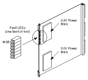
Each bank of LEDs displays forty-four status values and fifteen error values. The values are displayed by the banks as a binary number, with the most significant bit represented by the topmost LED (as viewed from the front of the cardcage). There are two types of messages:
Status codes (constant values). These are indicated by constantly lit LEDs, and the error messages are prefixed with PLED (which stands for PROM LED).
Error codes (flashing values). These are indicated by flashing LEDs, and the error messages are prefixed with FLED (which stands for flashing LED).
Status codes are displayed as the system progresses through the power-on tests and the LEDs stay lit for each state the system passes through. Because the LEDs stay lit (as opposed to flashing), status codes are also known as "constant values." To determine the system's state, note the pattern of lit LEDs and use one of the following sections to determine the status (constant) value and corresponding error code: For IP19 systems, see Section 5.7.1, "IP19 LED Status Codes." For IP21 systems, see Section 5.7.3, "IP21 LED Status Codes."
Error codes are displayed if a fatal error prevents the power-on tests from completing. The LEDs will flash the error value until the system is powered down or reset. Error codes have the prefix "FLED" (Flashing LED) attached to their descriptions. For IP19 systems, see Section 5.7.2, "IP19 LED Error Codes." For IP21 systems, see Section 5.7.4, "IP21 LED Error Codes."
These binary error codes apply to all of the microprocessors resident on the board. IP19 boards are configured with all four banks of LEDs, regardless of the number of microprocessors installed. See Table 5-5.
.
Table 5-5. IP19 Board Test Status LED Codes
LED Pattern Displayed | Description |
|---|---|
LSB X O O O O O MSB | PLED_CLEARTAGS (1) - Clearing the primary data cache tags. |
LSB O X O O O O MSB | PLED_CKCCLOCAL (2) - Testing CC chip local registers. |
LSB X X O O O O MSB | PLED_CCLFAILED_INITUART (3) - Failed the local test but trying to initialize UART. |
LSB O O X O O O MSB | PLED _CCINIT1 (4) - Initializing the CC chip local registers. |
LSB X O X O O O MSB | PLED_CKCCCONFIG (5) - Testing the CC chip config registers (requires usable bus to pass). If test hangs, usually means bus has failed. Check oscillator. |
LSB O X X O O O MSB | PLED_CCLFAILED_INITUART (6) - Failed the config reg test but trying to initialize UART. |
LSB X X X O O O MSB | PLED_NOCLK_INITUART (7) - CC clock not running. Init UART anyway. |
LSB O O O X O O MSB | PLED_CCINIT2 (8) - Initializing the CC chip config registers. |
LSB X O O X O O MSB | PLED_UARTINIT (9) - Initializing the CC chip UART. If test hangs, usually means bad UART clock. Check connections to System Controller. |
LSB O X O X O O MSB | PLED_CCUARTDONE (10) - Finished initializing the CC chip UART. |
LSB X X O X O O MSB | PLED_CKACHIP (11) - Testing the A chip registers. |
LSB O O X X O O MSB | PLED_AINIT (12) - Initializing the A chip. |
LSB X O X X O O MSB | PLED_CKEBUS1 (13) - Checking the Ebus with interrupts. |
LSB O X X X O O MSB | PLED_SCINIT (14) - Initializing the System Controller. |
LSB X X X X O O MSB | PLED_BMARB (15) - Arbitrating for a bootmaster. |
LSB O O O O X O MSB | PLED_BMASTER (16) - This processor is the bootmaster. |
LSB X O O O X O MSB | PLED_CKEBUS2 (17) - Running second Ebus test. Run only by the bootmaster. |
LSB O X O O X O MSB | PLED_POD (18) - Setting up this CPU slice for POD mode. |
LSB X X O O X O MSB | PLED_PODLOOP (19) - Entering POD loop. |
LSB O O X O X O MSB | PLED_CKPDCACHE1 (20) - Checking the primary data cache. |
LSB X O X O X O MSB | PLED_MAKESTACK (21) - Creating a stack in the primary data cache. |
LSB O X X O X O MSB | PLED_MAIN (22) - Jumping into C code - calling main. |
LSB X X X O X O MSB | PLED_CKIAID (23) - Checking IA and ID chips on master IO4. |
LSB O O O X X O MSB | PLED_CKEPC (24) - Checking EPC chip on master IO4. |
LSB X O O X X O MSB | PLED_IO4INIT (25) - Initializing the IO4 PROM. |
LSB O X O X X O MSB | PLED_NVRAM (26) - Getting NVRAM variables. |
LSB X X O X X O MSB | PLED_FINDCONS (27) - Checking the path to the EPC chip, which contains the console UART. |
LSB O O X X X O MSB | PLED_CKCONS (28) - Testing the console UART. |
LSB X O X X X O MSB | PLED_CONSINIT (29) - Setting up the console UART. |
LSB O X X X X O MSB | PLED_CONFIGCPUS (30) - Configuring out CPUs that are disabled. |
LSB X X X X X O MSB | PLED_CKRAWMEM (31) - Checking raw memory (running Board Internal Self-Test [BIST]. |
LSB O O O O O X MSB | PLED_CONFIGMEM (32) - Configuring memory. |
LSB X O O O O X MSB | PLED_CKMEM (33) - Checking configured memory. |
LSB O X O O O X MSB | PLED_WTCONFIG (34) - Writing evconfig structure: The bootmaster CPU writes the entire array. The slave CPUs only write their own entries. |
LSB X X O O O X MSB | PLED_LOADPROM (35) - Loading IO4 PROM. |
LSB O O X O O X MSB | PLED_CKSCACHE1 (36) - First pass of secondary cache testing. Tests the scache like a RAM. |
LSB X O X O O X MSB | PLED_CKPICACHE (37) - Checking the primary instruction cache. |
LSB O X X O O X MSB | PLED_BADEAROM (38) - The EAROM associated with the CPU is corrupt and couldn't be repaired. |
LSB X X X O O X MSB | PLED_CKSCACHE2 (39) - Checking secondary data cache writeback mechanism. |
LSB O O O X O X MSB | PLED_CKBT (40) - Check the bus tags. |
LSB X O O X O X MSB | PLED_BTINIT (41) - Clearing the bus tags. |
LSB O X O X O X MSB | PLED_CKPROM (42) - Checksumming the I/O PROM. |
LSB X X O X O X MSB | PLED_INSLAVE (43) - This CPU is entering slave mode. |
LSB O O X X O X MSB | PLED_PROMJUMP (44) - Jumpering to the I/O PROM. |
LSB X O X X O X MSB | PLED_SLAVEJUMP (45) - A slave is jumping to the IO4 PROM slave code. |
Table 5-6 lists the IP19 board power-on test failure LED codes.
Table 5-6. IP19 Board Power-on Test Failure LED Codes
LED Pattern Displayed | Description (Flashing Value Displayed) |
|---|---|
LSB O X X X O X MSB | FLED_CANTSEEMEM (46) - Flashed by slave processors if they take an exception while trying to write their evconfig entries. Often means that processor is getting D-chip parity errors. |
LSB X X X X O X MSB | FLED_NOUARTCLK (47) - The CC UART clock is not running. No System Controller access possible. |
LSB O O O O X X MSB | FLED_INPOSSIBLE1 (48) - System fell through an unreturning subroutine (shouldn't be possible). |
LSB X O O O X X MSB | FLED_DEADCOP1 (49) - Coprocessor 1 is dead (no error does not mean coprocessor is good). |
LSB O X O O X X MSB | FLED_CCCLOCK (50) - Cache controller (CC) clock is not running. |
LSB X X O O X X MSB | FLED_CCLOCAL (51) - Failed CC local register tests. |
LSB O O X O X X MSB | FLED_CCCONFIG (52) - Failed CC config register tests. |
LSB X O X O X X MSB | FLED_ACHIP (53) - Failed A chip register tests. |
LSB O X X O X X MSB | FLED_BROKEWB (54) - By the time this CPU arrived at bootmaster arbitration barrier, the rendezvous time had passed. CPU is running too slowly, the ratio of the bus clock rate to CPU clock rate is too high, or a bit in the CC clock is stuck on. |
LSB X X X O X X MSB | FLED_BADCACHE (55) - CPU's primary data cache test failed. |
LSB O O O X X X MSB | FLED_BADIO4 (56) - IO4 board is bad (can't get to console). |
LSB X O O X X X MSB | FLED_UTLBMISS (57) - Took a TLB refill exception. |
LSB O X O X X X MSB | FLED_XTLBMISS (58) - Took an extended TLB refill exception. |
LSB X X O X X X MSB | FLED_CACHE (59) - Unused. |
LSB O O X X X X MSB | FLED_GENERAL (60) - Took a general exception. |
LSB X O X X X X MSB | FLED_NOTIMPL (61) - Took an unimplemented exception. |
LSB O X X X X X MSB | FLED_ECC (62) - Took a cache error exception. |
Table 5-7 lists the IP21 status codes:
Table 5-7. IP21 Board Test Status LED Codes
LED Pattern Displayed | Description (Constant Value Displayed) |
|---|---|
LSB X O O O O O MSB | PLED_STARTUP 1 (1) - PROM has started execution |
LSB O X O O O O MSB | PLED_TESTICACHE (2) - test icache |
LSB X X O O O O MSB | PLED_CHKSCACHESIZE (3) - check scache size |
LSB O O X O O O MSB | PLED_INITCOP0 (4) - init cop0 registers |
LSB X O X O O O MSB | PLED_FLUSHTLB (5) - flush tlb |
LSB O X X O O O MSB | PLED_FLUSHSAQ (6) - flush store address queue |
LSB X X X O O O MSB | PLED_CLEARTAGS (7) - Clearing the pd tags |
LSB O O O X O O MSB | PLED_CKCCLOCAL (8) - Testing CC chip local registers |
LSB X O O X O O MSB | PLED_CCLFAILED_INITUART (9) - Failed the local test but trying to initialize the UART anyway |
LSB O X O X O O MSBLSB X X O X O O MSB | PLED_CCINIT1(10), PLED_CKCCCONFIG (11) - Testing the CC config registers requires a usable bus to pass) Hanging in this test usually means that the bus has failed. Check the oscillator. |
LSB O O X X O O MSB | PLED_CCCFAILED_INITUART (12) - Failed the config reg test but trying to initialize the UART anyway |
LSB X O X X O O MSB | PLED_NOCLOCK_INITUART (13) - CC clock isn't running init uart anyway |
LSB O X X X O O MSB | PLED_CCINIT2 (14) - Init CC chip config registers |
LSB X X X X O O MSB | PLED_UARTINIT (15) - Init CC chip UART. Hanging in this test usually means that the UART clock is bad. Check the connection to the system controller. |
LSB O O O O X O MSB | PLED_CCUARTDONE (16) - Finished initializing the CC chip UART |
LSB X O O O X O MSB | PLED_CKACHIP (17) - Testing A chip registers |
LSB O X O O X O MSB | PLED_AINIT (18) - Initializing the A chip |
LSB X X O O X O MSB | PLED_CKEBUS1 (19) - Checking the EBus with interrupts. |
LSB O O X O X O MSB | PLED_SCINIT (20) - Init system controller |
LSB X O X O X O MSB | PLED_BMARB (21) - Arbitrating for a bootmaster |
LSB O X X O X O MSB | PLED_BMASTER (22) - This processor is the bootmaster |
LSB X X X O X O MSB | PLED_CCJOIN (23) - Test CC join register |
LSB O O O X X O MSB | PLED_WG (24) - Test write gatherer register & buffer |
LSB X O O X X O MSB | PLED_POD (25) - Setting up this CPU slice for POD mode |
LSB O X O X X O MSB | PLED_PODLOOP (26) - Entering POD loop |
LSB X X O X X O MSB | PLED_CKPDCACHE1 (27) - Checking the pd cache |
LSB O O X X X O MSB | PLED_MAKESTACK (28) - Creating a stack in the primary data cache |
LSB X O X X X O MSB | PLED_MAIN (29) - Jumping into C code - calling main() - |
LSB O X X X X O MSB | PLED_LOADPROM (30) - Loading IO4 prom |
LSB X X X X X O MSB | PLED_CKSCACHE1 (31) - First pass of secondary cache testing - test the scache like a RAM |
LSB O O O O O X MSB | PLED_CKBT (32) - Check the bus tags |
LSB X O O O O X MSB | PLED_INSLAVE (33) - This CPU is entering slave mode |
LSB O X O O O X MSB | PLED_PROMJUMP (34) - Jumping to the IO prom |
LSB X X O O O X MSB | PLED_NMIJUMP (35) - Jumping through the NMIVEC |
LSB O O X O O X MSB | PLED_WRCONFIG (36) - Writing evconfig structure: The master CPU writes the whole array. The slaves only write their own entries. |
LSB O O O X X X MSB | PLED_SCACHE_TAG_ADDR (56) |
LSB X O O X X X MSB | PLED_SCACHE_TAG_DATA (57) |
LSB O X O X X X MSB | PLED_SCACHE_ADDR (58) |
LSB X X O X X X MSB | PLED_SCACHE_DATA (59) |
LSB O O X X X X MSB | PLED_SCACHE_INIT (60) |
LSB X O X X X X MSB | PLED_SCACHE_INIT (61) |
Table 5-8 lists the IP21 board power-on test failure LED codes:
Table 5-8. IP21 Board Power-On Test Failure LEDs
LED Pattern Displayed | Description |
|---|---|
LSB X O X O O X MSB | FLED_ICACHE_FAIL (37) |
LSB O X X O O X MSB | FLED_CANTSEEMEM (38) - Flashed by slave processors if they take an exception while trying to write their evconfig entries. Often means the processor's getting D-chip parity errors. |
LSB X X X O O X MSB | FLED_SCACHE_SIZE_INCONSISTENT (39) - Scache size is inconsistent |
LSB O O O X O X MSB | FLED_IMPOSSIBLE1 (40) - We fell through one of the supposedly unreturning subroutines. Really shouldn't be possible. |
LSB X O O X O X MSB | FLED_DEADCOP1 (41) - Coprocessor 1 is dead - not seeing this doesn't mean it works. |
LSB O X O X O X MSB | FLED_CCCLOCK (42) - Failed CC local register tests. |
LSB X X O X O X MSB | FLED_CCLOCAL (43) - Failed CC local register tests. |
LSB X O X X O X MSB | FLED_ACHIP (45) - Failed A Chip register tests |
LSB O X X X O X MSB | FLED_BROKEWB (46) - By the time this CPU had arrived at the bootmaster arbitration barrier, the rendezvous time had passed. This implies that a CPU is running too slowly, the ratio of bus clock to CPU clock rate is too high, or a bit in the CC clock is stuck on. |
LSB X X X X O X MSB | FLED_BADDCACHE (47) - This CPU's primary data cache test failed |
LSB O O O O X X MSB | FLED_BADIO4 (48) - The IO4 board is bad - can't get to the console. |
LSB X O O O X X MSB | FLED_UTLBMISS (49) - Took a TLB Refill exception |
LSB O X O O X X MSB | FLED_KTLBMISS (50) - Took a kernel TLB Refill exception |
LSB X X O O X X MSB | FLED_BADEAROM (51) - Scache test 2 doesn't exist, so replace it with FLED_BADEAROM. The EAROM was corrupted and couldn't be repaired. |
LSB O O X O X X MSB | FLED_GENERAL (52) - Took a general exception |
LSB X O X O X X MSB | FLED_NOTIMPL (53) - Took an unimplemented exception |
LSB O X X O X X MSB | FLED_SCACHE_SIZE_WRONG (54) - Bad scache size |
LSB X X X O X X MSB | FLED_SCACHE_TAG_JUMPER (55) |
LSB O O O X X X MSB | PLED_SCACHE_TAG_ADDR (56) |
LSB X O O X X X MSB | PLED_SCACHE_TAG_DATA (57) |
LSB O X O X X X MSB | PLED_SCACHE_ADDR (58) |
LSB X X O X X X MSB | PLED_SCACHE_DATA (59) |
LSB O O X X X X MSB | PLED_SCACHE_INIT (60) |
LSB X O X X X X MSB | PLED_SCACHE_INIT (61) |
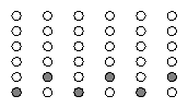
When the Power-on Diagnostics (POD) are running, a pair of LEDs from each bank of processor LEDs will flash alternately. After POD runs and the system enters the PROM monitor, the LEDs on the bootmaster CPU will display a fixed value (decimal 18, binary 010010). All other slave processors will loop on a pattern waiting for a command (see Figure 5-10).

The bootmaster CPU will loop on the pattern shown in Figure 5-11 when polling the CC UARTs.
This section describes the commands used to verify and/or change the system configuration using the IO4 Boot PROM Monitor.
Check the current system configuration using either the hinv command, or two variations of it: hinv -b and hinv -b -v:
hinv performs exactly as it did in previous releases.
hinv -b is similar to the info command in POD and provides additional information, such as: the number of processors present, the amount of memory installed, and whether or not an IO4 board is present.
hinv -b -v supplies additional information about each processor, memory bank, and I/O adapter.
Modify the system configuration using the enable and disable commands:
enable x y, where x is the board slot number and y is the memory bank number, turns on the selected memory bank on the MC3 board. The disable command works in the same way.
enable x y, where x is the cardcage slot number and y is the CPU number, turns on the selected processor on the IP19 board. The disable command works in the same way. Entering enable x, without specifying the CPU, number turns on every CPU resident in the specified cardcage slot.
| Note: The system must be power-cycled following an enable command, in order for the new configuration to be activated. The disable command does not require the system to be power-cycled. |
Change the system configuration and then power-cycle the system. Enter one of the hinv commands. The current configuration is compared to the stored hardware inventory, and any variations are flagged.
Revise the stored hardware inventory to reflect the new configuration by entering update. This command rewrites the stored hardware inventory locations in the IO4 board's NVRAM.
This section describes how to reconfigure the system to boot from a different system disk.
Bring up the System Maintenance menu.
Type 5 to enter the Command Monitor.
Type printenv to display the following screen:
>> printenv
SystemPartition=scsi(0)disk(1)partition(8)
OSLoadPartition=scsi(0)disk(1)partition(0)
AutoLoad=No
dbgtty=multi(0)serial(0)
root=dks0d1s0
nonstop=0
rbaud=19200
TimeZone=PST8PDT
console=d
diskless=0
dbaud=9600
sgilogo=y
netaddr=192.48.150.68
ConsoleOut=multi(0)serial(0)
ConsoleIn=multi(0)serial(0)
cpufreq=50
| Note: The lines in bold contain the values that must be changed before the system will boot from the new disk. In this example, the address of the new system disk is "4." |
Use the setenv command to enter the following information:
>> setenv systempartition dksc(0,4,8)
>> setenv osloadpartiton dksc(0,4,0)
>> setenv root dks0d4s0
>> single
The system will begin to boot in single-user mode.