This chapter provides a functional overview of the Everest board set. Each of the boards making up the Everest board set is described, as well as the optional mezzanine boards, the VCAM, the I/O panel filter boards, and the SCSI channel configuration boards. Functional overviews of the RealityEngine2 and VTX graphics board sets are also provided in this chapter.
Figure 2-1 is a simplified block diagram of the Everest graphics workstation. The primary differences between the server and the graphics workstation are their respective midplanes and the installed boards.
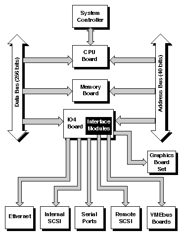
The Everest board set comprises the IP19 CPU board, the MC3 memory board, the IO4 Interface board, and a VCAM board. Additionally, a number of optional mezzanine boards can be attached to the IO4 board. All of these boards are described in detail in the following sections.
The principal features of the Everest board set are:
Four R4400 microprocessors per CPU board (maximum)
1200 MB/second, 256-bit system data bus
40-bit address bus
Address and data bus interface application-specific integrated circuits (ASICs) on each board
Can support a single VTX subsystem or multiple RealityEngine2 (RE2) graphics subsystems
Can support up to 2 GB of interleaved memory per memory board
Supplies dual 8- or 16-bit SCSI channels for each SCSIBox 2
Additional Flat Cable Interface (FCI), VMEbus, and SCSI ports available on optional Interface Modules
The IO4 board (described in Section 2.4.1, "IO4 Board") provides a single Ethernet AUI connection. However, the design of the Everest system allows for the following additional network solutions:
native VMEbus network boards
network boards attached to the F mezzanine connectors
a VME network board attached through the flat-cable interface (FCI)
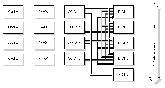
The IP19 is a multiprocessor CPU board that supports two or four R4400 microprocessors. The board logic is divided or "sliced" so that each of the microprocessors has its own dedicated supporting logic, which allows each microprocessor to run independently of the others. The only portion of the CPU board circuitry that is shared by the resident microprocessors is the bus arbitration logic. See Figure 2-2 for a functional block diagram illustrating the IP19 board.
Note that each microprocessor has its own cache and cache controller (CC Chip), but shares the Address (A Chip) and Data (D Chip) ASICs that provide the interface to the system (Everest) bus.
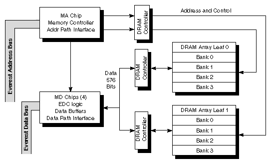
The Everest Memory Board (MC3) can support 32 DRAM SIMMs of either 16 or 64 MB. The minimum configuration is 64 MB and the maximum is 2 GB. The memory is arranged in 2 arrays of 4 banks each. Each bank has 144 four-bit wide DRAMs.
The MC3 communicates with the Everest bus through a series of ASICs. The Memory Address (MA) chip provides the interface between the memory array and the Everest address bus. This gate array includes bus arbitration logic, decode logic, and a pair of DRAM controllers.
Each DRAM controller generates the memory address and control lines needed to control two banks of DRAMs. These outputs are driven to the memory arrays through a single level of buffers. Control signals are also generated for the Memory Data ASICs (MD Chips).
The four MD Chips provide data buffering and error detection/correction for information transferred between the 576-bit memory array and the 256-bit Everest data bus. Each of these identical chips drives one quarter of the data bus. These ASICs are controlled by the MA Chip and perform no operations independently, except for notifying the MA Chip when an error has been detected.
Interleaving is supported between array leafs of equal memory size on the same board and between two or more memory boards with the same total memory capacity. A fully populated memory board uses two-way on-board interleaving. Two or four memory boards can be configured for up to eight-way interleaving. Figure 2-3 is a functional block diagram of the MC3 board.
The I/O subsystem consists of an IO4 board, a VCAM board, and some combination of optional plug-in mezzanine boards. Mezzanine boards include two types of FCI board, and a SCSI board.
The following sections describe the IO4 board and the mezzanine boards.
The IO4 board supplies the system with a basic set of I/O controllers, including:
three RS-232 ports
one RS-422 port
one AUI Ethernet connector
a second-level boot flash EPROM
a bi-directional parallel port
NVRAM used to store system configuration information
two Flat Cable Interfaces (FCIs)
two SCSI-2 cable connections
Communication with the VME and SCSI buses, the installed graphics boards set(s), and the network are managed by a set of interface control chips. Two Flat Cable Interface (FCI) Controller chips (F Chips) handle the data transfers to and from any internal graphics board sets (if installed), and any VMEbus boards. The SCSI-2 Controller chip (S1) serves as an interface to the various SCSI-2 buses. The Everest Peripheral Controller (EPC) chip manages the data movement to and from the Ethernet, a parallel port, and various types of on-board PROMs and RAM. See Figure 2-4 for a functional block diagram of the IO4 board.
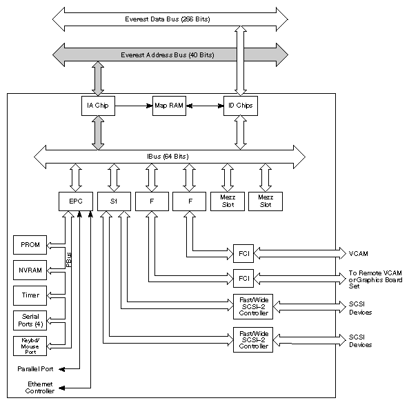
Chips on the IO4 board include the following:
| F Chip |
The F chip is always designated the slave on the FCI. The VME Cache Controller (VMECC) or the Flat Cable to Graphics (FCG), at the other end of the FCI, is always the master. The VMECC is the interface between the FCI and the VMEbus or HIPPI network board. The FCG connects the FCI to the graphics subsystem. | |
| S1 Chip |
| |
| EPC Chip |
Both the network controller and the parallel port have DMA controllers built into the EPC to provide the necessary support. The only access to the PBus devices is through load/store instructions performed by one of the CPUs. In addition, the PBus devices have ten independent interrupt lines. |
The I/O Interface Modules, or mezzanine boards, can provide the IO4 board with a variety of additional bus interfaces, network interfaces, and serial ports. The interface modules mount directly to the IO4 board. Brief descriptions of the available interface modules are provided in the following sections.
| SCSI Mezzanine (S Mezz) Board |
| |
| Flat Cable Interface (F Mezz) Boards |
| |
| VMEbus Channel Adapter Module (VCAM) |
|
Table 2-1 lists the mezzanine boards and the supported configurations. Note that these are the only restrictions on the available configurations: the VCAM must be installed on the first (or only) IO4 board, and a standard-length F mezz board will not physically fit on an IO4 board that already has a VCAM mounted.
Table 2-1. Supported IO4, VCAM and Mezzanine Board Configurations
Host Board | VCAM | S Mezz (SCSI-I) | S Mezz (SCSI-II) | F Mezz | F Mezz (short) |
|---|---|---|---|---|---|
IO4 (first or only) | Yes | Yes | Yes | No | Yes |
IO4 (additional) | No | Yes | Yes | Yes | Yes |
The SCSI channel adapter boards configure the available SCSI channels on an IO4 board as either single-ended or differential. These boards mount directly to the IO4 board SCSI channel connectors and are color-coded. Table 2-2 shows the color-coding scheme:
Table 2-2. SCSI Channel Adapter Board Color-coding Scheme
SCSI Channel Adapter Board Color | Signal Configuration |
|---|---|
Green | Single-ended |
Red | Differential |
Power boards are DC-to-DC converters that take the 48 VDC from the system midplane and step it down to levels appropriate for the buses, circuit boards, and SCSI drives. Four types of power board are used with the rackmount systems:
The System Controller board supplies +1.5 VDC at 30 amps for use by the EBus. This board also provides power for the microprocessor on the System Controller and for the LCD display on the system status panel.
The 505 power board generates +5 VDC at 80 amps for use by the boards. There is a single and a dual version of the 505 board; the dual version has two power bricks.
The 512 power board generates +5 VDC at 40 amps and +12 VDC at 17 amps for the VMEbus.
The 512S power board provides +5 VDC at 40 amps and +12 VDC at 17 Amps for the SCSI drive box.
The System Controller, 505, and 512 power boards are available both with and without extender boards. Used with extenders, the power boards are installed in cardcage 1 and supply the necessary voltages to the midplane. Used without extenders, these boards are attached directly to the front of the optional cardcage 3 backplane. The 512S is designed to attach to the SCSI backplane in the SCSIbox.
The RealityEngine2 (RE2) and VTX graphics subsystems consist of three board types: the Geometry Engine (GE10 or GE10V), the Display Generator (DG2), and the Raster Memory (RM4) board.
The RE2 board set uses a GE10 with 12 geometry engine processors installed. A maximum of 4 RM4 boards are supported, along with a 21-inch color monitor.
The VTX board set uses a GE10V with 6 geometry engine processors installed. The VTX supports a single RM4 board and a 19-inch color monitor.
The principal features of the RE2 and VTX graphics board sets are:
greater texel storage capacity (4 MB versus 256 KB in PowerVision)
more color and greater depth and spatial resolution
RGB and simultaneous low-resolution composite video out
supports most video standards, such as PAL, NTSC and HDTV (RE2 only)
built-in genlocking
greater z-buffering capability (32 bits versus 24 bits in PowerVision)
supports full scene antialiasing (1K x 1K)
80 megapixels per second (Mpps) with 5-span system
160 megapixels per second with 10-span system
real-time texture mapping
antialiasing for polygons, vectors, and points
quad buffering for interactive high-resolution stereoscopy
hardware support for image processing
standard NTSC/PAL/M ppsM/ppsSVHS output
broadcast-quality video options available
stereo in a window
ultra-high quality color: 12 bits per component (48-bit RBGA, quad-buffered)
The primary board in both graphics subsystems is the GE10. The GE10 interfaces with the host system through a Flat Cable Interface (FCI) on the IO4 board. The FCI is a 64-bit wide bus that has a maximum transfer rate of 160 MB per second. Its purpose is to provide an interface on the IO4 board between the graphics subsystems and the Ibus. The FCI leaves the IO4 board and passes through the VCAM to enter the system midplane. The GE10 is installed in a dedicated slot on the midplane, which is connected directly to the FCI.
The GE10 communicates with the RM4(s) over the Triangle bus and with the DG2 board over the Video Control (VC) bus. The Video Control bus provides access to the color maps, window display modes, and cursor control modes. Communication between the RM4(s) and the DG2 board is over the Video bus. See Figure 2-5 for a block diagram of the RE2/VTX board set.
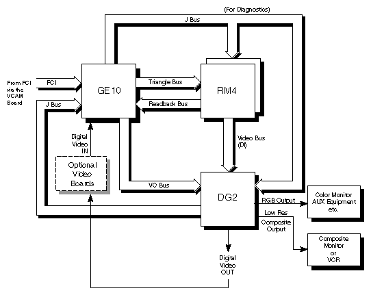
The RE2/VTX board set uses custom ASICs and parallel processing to reduce the amount of required hardware. This reduction can be seen when the RE2/VTX board set is compared to its predecessor, PowerVision. The RE2/VTX has three standard boards; PowerVision requires a minimum of four boards.
The Geometry Engine (GE10/GE10V) board processes Graphics Library® (GL) commands and data from the system CPU board and is the first stage of the graphics pipeline. There are two versions of the Geometry Engine:
The GE10 contains 12 geometry engine processors and is used in the RE2 board set.
The GE10V contains 6 geometry processors and is used in the VTX board set.
Figure 2-6 provides a block diagram that illustrates both versions of the Geometry Engine.
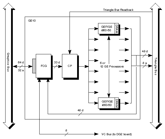
The following discussion of the Geometry Engine refers to the GE10 board. However, unless otherwise noted the information applies to both the GE10 and GE10V.
The GE10 typically receives vertex data defining the location, orientation, color, and texture mapping coordinates of a polygon. If the polygon has more than three vertices, the GE10 subdivides the polygon into triangles. Triangles are the basic polygonal working units of the system. Data output from the GE10 geometry subsystem passes over the Triangle bus to the raster memory subsystem (RM4 board(s)).
The major components on the GE10 are the flat cable interface to graphics (FCG) ASIC, the command processor (CP), and the Geometry Engine (GE) processors.
The FCG ASIC interfaces data from the FCI via the VCAM to the graphics pipeline and transmits the data to the CP. The CP acts as the central distributing point for the data and instructions and reorders the input stream for efficient processing. The CP distributes data to the GE processors over a 32-bit bus.
The RE2 GE10 has 12 GE processors. The VTX GE10V has 6 GE processors.The GE processors contain an Intel™ i860XP floating point microprocessor, a 64-bit wide DRAM (which stores both code and instructions), and the Geometry Engine FIFO (GEF) ASIC chip. The Intel microprocessor can perform 100 million floating point operations per second (MFLOPS). See Figure 2-7 for a block diagram of the GE processor.
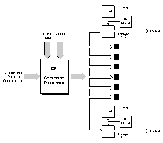
The GE10 ties into the display generator (DG2) board through the video control bus. This bus allows access to color maps, window display modes, cursor control as well as video format and timing control.
The Raster Memory (RM4) Board scans and converts triangle data from the triangle bus into pixel data. The RM4 then organizes the data into a series of spans (vertical strips of pixels) and transfers it to the frame buffer. Following the transfer to the frame buffer, the RM4 hands off control of the graphics subsystem to theDG2. The RM4 board is shown in Figure 2-8.
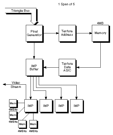
The RM4 board is composed of the following main components:
Pixel Generator (PG) ASIC
Texture Address (TA) ASIC
DRAM Texture Memory
Texture Data (TD) ASIC
Image Memory Processor (IMP) Buffer (IB) ASIC
To get pixels into the frame buffer, the pixel generators (PGs) must take the spans they have generated and redraw them from the top to the bottom pixel to find the parameter values for each of the polygon's interior pixels.
Triangles feed into five parallel pixel generators. The PGs walk the top and bottom edges of the triangles, identifying which pixels lie along those edges. For each x location in the pixel (or subpixel) grid, a pair is formed from the top and bottom pixels touched by each polygon. Each of the pixels in the span pair are then assigned parameters from the vertices of the polygon.
Two pixel data paths from the pixel generators facilitate the processing performance. One path processes the pixels for texture mapping. The other path bypasses texture processors to render non-textured primitives. If a pixel requires texture processing, the PGs calculate the texture coordinates of the pixel. This information goes to the Texture Address (TA) ASIC, which calculates the texture address information for texture memory.
The TD ASIC resamples the texture data. It resamples eight values for each pixel. Data is then sent to the Image Memory Processor (IMP) Buffer (IB), which distributes the data to the four IMP chips.
If no texture processing is required, the pixel goes straight to the IMP buffer. Once the IB creates the blended color, the pixel goes to one of four parallel image engine processors, which then passes the pixel to one of four image memory processors (IMPs).
 | Note: Each raster memory board has 20 IMPs. Each IMP contains four image engines, so there are 80 image engines per board. |
The main responsibilities of the IMPs are as follows:
filter the subpixel rendered image into the actual displayable frame buffer
filter the subpixel z-buffer data
decide whether to write the pixel based upon the z-buffer value
perform the alpha blending of each new pixel with the pixel value that has already been rendered at the same location
send the digital pixels to the display generator subsystem (DG2) over the pixel bus
The cost-reduced VTX supports one RM4 board. The RE2 board set can have up to four RM4 boards per pipeline. As more RM4 boards are added, the spans are interleaved, providing higher resolution and display quality. A 10-span system has 10 pixel generators, 160 image engines, and memory.
To differentiate the boards, the RM4s receive a 2-bit identity field from the video bus front plane, the DI1 (for pipeline 0) or the DI2 (for pipeline 1). This field identifies which of four addresses a board occupies.
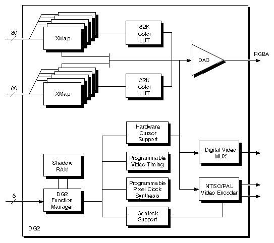
The DG2 board receives digital frame buffer pixel data from the RM4 board over the video bus. The DG2 processes the pixel data through digital-to-analog converters (DACs) to generate an analog pixel stream for display. The principal components of the DG2 board are the XMAP ASICs, the function manager ASIC, and an NTSC/PAL encoder. See Figure 2-9 for a functional block diagram of the DG2 board.
| XMAP ASICs |
| |
| DG2 Function Manager |
cursor display video timing pixel clock genlocking The function manager also contains the HLIST and VLIST display parameters that provide horizontal and vertical pixel display codes. The video input format (VIF) processor, in the function manager, generates the video pixel clock time base. The processor can operate in free-running or in externally genlocked mode for synchronization. In genlock mode, the VIF syncs on an external source. A video output format (VOF) processor in the function manager enables a master sync source to loop through the system (Genlock Out) to other equipment. The shadow RAM or SRAM stores previous display data to help support windowing. | |
| NTSC/PAL Encoder |
|