This chapter describes how to install the VME Sync board upgrade into the
CHALLENGE L (deskside) and XL (rackmount) systems.
Installation consists of the following major steps:
verifying the kit contents
checking the jumper and DIP switch settings on the board
removing the RS-232 PROMs and installing daughter boards (if required)
installing the VME Sync board into a system
jumpering the backplane (if a VME slot or slots are skipped)
connecting the board to the I/O panel
installing software
verifying installation
Figure 2-1 shows the major components for the VME Sync board upgrade (marketing code, C8-VMESYNC). The marketing codes for the different interfaces are:
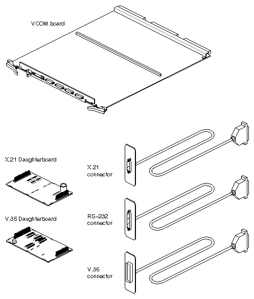
The VME Sync board should already be configured with the correct jumper settings and DIP switch selections (see note below). However, you should double check the settings as outlined in this section.
 | Note: DIP switches 7 and 8 may need to be changed. These switches are preset for a board address of 0 (a single VME Sync board configuration). See Table 2-27 for additional information. |
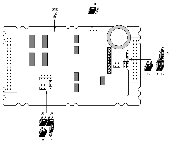
Figure 2-2 illustrates the proper VME Sync board jumpering and Table 2-13 describes the jumper functions.
Figure 2-2. VME Sync Board With Required Jumper and DIP Switch Settings (Board 0 Configuration Shown)
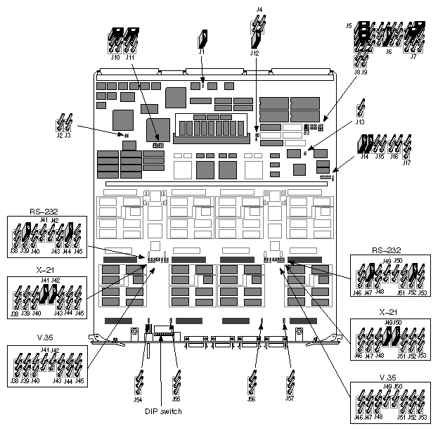 |
| Note: Jumper blocks J18 through J37 do not exist on the board. Their positions are reserved for possible future use. |
Table 2-1. Jumper Description - J1
Jumper Number/Name | Function |
|---|---|
J1–Mailbox Reset | When jumpered, it allows the host CPU to reset the VME Sync board by writing to a mailbox register in the VSAM device (an ASIC that helps provide the VMEbus interface.)
|
See Figure 2-3 |
|

Table 2-2. Jumper Description - J2
Jumper Number/Name | Function |
|---|---|
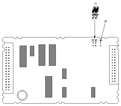
J2–Asserting SYSRESET to the VMEbus | When jumpered, it allows a local reset (from the VME Sync board) to reinitialize the VMEbus. |
See Figure 2-4 |
|

Table 2-3. Jumper Description - J3
Jumper Number/Name | Function |
|---|---|
J3–Cache Disable | When not jumpered, it enables the on-chip cache memory of the 68020 so that a copy of recently executed instructions and most recently accessed data is retained. This is potentially useful in shortening processing time, as re-executed instructions may not need to be fetched from program memory. |
See Figure 2-5 |
|
Table 2-4. Jumper Description - J4
Jumper Number/Name | Function |
|---|---|
J4–Watchdog Timeout Function | This header provides a means of monitoring the software integrity on the VME Sync board. The 68020 must refresh the watchdog timer on a regular basis; if it does not, a timeout will occur and the SYSFAIL LED will go on. When jumpered, it either causes the 68020 to halt or cause a full reset of the VME Sync board. No jumper indicates that a timeout has no effect on the VME Sync hardware. The board will then attempt to continue operation. |
See Figure 2-6 |
|

Table 2-5. Jumper Descriptions - J5, J6
Jumper Number/Name | Function |
|---|---|
J5, J6–EPROM Bank 1 Device Selection | These two jumper blocks (J5 and J6) indicate the size and type of PROM or RAM devices installed at the bank 1 location. The Silicon Graphics configuration has a 32K x 8 EPROM. |
See Figure 2-7 |
|
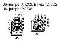
Table 2-6. Jumper Description - J7
Jumper Number/Name | Function |
|---|---|
J7–EPROM Bank 0 Device S election | This jumper block indicates the size and device type of the EPROM installed at bank 0. The Silicon Graphics board version has a 64K x 8 EPROM at this location. |
See Figure 2-8 |
|

Table 2-7. Jumper Description - J8
Jumper Number/Name | Function |
|---|---|
J8–COM device Interrupt Priority Scheme | When not jumpered, it sets up a round-robin priority scheme to determine the order that the VBIC handles interrupt requests. The VBIC is paired with the VSAM to provide the VMEbus interface for the board |
See Figure 2-9 |
|
Table 2-8. Jumper Description - J9
Jumper Number/Name | Function |
|---|---|
J9–COM Port Interrupt Enable | This header sets the number of ports that can issue interrupt requests to the VBIC interrupt controller to either four (no jumper) or eight (with jumper). The VME Sync board is set for four ports. |
See Figure 2-10 |
|
Table 2-9. Jumper Descriptions - J10, J11
Jumper Number/Name | Function |
|---|---|
J10, J11–Device Speed | These two headers set the maximum access speed and minimum write pulse. The VME Sync board is set for an access speed of 250 ns and a minimum write pulse of 150 ns. |
See Figure 2-11 |
|
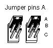
Table 2-10. Jumper Description - J12
Jumper Number/Name | Function |
|---|---|
J12–Local Bus Timeout Disable | When jumpered, it enables a local bus timeout to avoid locking up the processor due to programming error or hardware failure. |
See Figure 2-12 |
|
Table 2-11. Jumper Description - J13
Jumper Number/Name | Function |
|---|---|
J13–VMEbus System Controller | When not jumpered, it assumes that the VME Sync board will not be configured as the VMEbus system controller. |
See Figure 2-13 |
|
Table 2-12. Jumper Descriptions - J14 through J17, J18 through J37
Jumper Number/Name | Function |
|---|---|
J14 throughJ17–Diag Port Configuration (not used) | Not applicable |
J18 through J37 | These jumper blocks do not exist on the board and are reserved for future use. |
Table 2-13. Jumper Descriptions - J38, J39
Jumper Number/Name | Function |
|---|---|
J38, J39–Transmit Clock Source | These jumper blocks set the transmit clock source for channel 3 from the receive clock for RS-232 operation. |
See Figure 2-14 |
|

Table 2-14. Jumper Description - J40
Jumper Number/Name | Function |
|---|---|
J40–SYNC Input to the 85C30 | The 85C30 serial communications controller has one SYNC input for each channel. No jumper indicates that the SYNC input is not connected. |
See Figure 2-15 |
|

Table 2-15. Jumper Descriptions - J41, J42
Jumper Number/Name | Function |
|---|---|
J41, J42–Jumpering for X.21 Module | These headers enable the software to determine if an X.21 module is installed or not. No jumpers indicate that an X.21 module is not installed. However, jumpers must be installed at this location for X.21 operation. |
See Figure 2-16 |
|
Table 2-16. Jumper Description - J43
Jumper Number/Name | Function |
|---|---|
J43–SYNC Input to the 85C30 | The 85C30 serial communications controller has one SYNC input for each channel. No jumper indicates that the SYNC input is not connected. |
See Figure 2-17 |
|
Table 2-17. Jumper Descriptions - J44, J45
Jumper Number/Name | Function |
|---|---|
J44, J45–Transmit Clock Source | These jumper blocks set the transmit clock source for the channel 2 port on the board. These jumpers indicate that the port will receive the transmit clock on pins 12 and 15 of the 34-pin connector. |
See Figure 2-18 |
|

Table 2-18. Jumper Descriptions - J46, J47
Jumper Number/Name | Function |
|---|---|
J46, J47–Transmit Clock Source | These jumper blocks set the transmit clock source for the channel 1 port on the board. These jumpers indicate that the port will receive the transmit clock on pins 12 and 15 of the 34-pin connector. |
See Figure 2-19 |
|

Table 2-19. Jumper Description - J48
Jumper Number/Name | Function |
|---|---|
J48–SYNC Input to the 85C30 | The 85C30 serial communications controller has one SYNC input for each channel. No jumper indicates that the SYNC input is not connected. |
See Figure 2-20 |
|
Table 2-20. Jumper Descriptions - J49, J50
Jumper Number/Name | Function |
|---|---|
J49, J50–Jumpering for X.21 Module | These headers enable the software to determine if an X.21 module is installed or not. No jumpers indicate that an X.21 module is not installed. However, jumpers must be installed at this location for X.21 operation. |
See Figure 2-21 |
|
Table 2-21. Jumper Description - J51
Jumper Number/Name | Function |
|---|---|
J51–SYNC Input to the 85C30 | The 85C30 serial communications controller has one SYNC input for each channel. No jumper indicates that the SYNC input is not connected. |
See Figure 2-22 |
|
Table 2-22. Jumper Descriptions - J52, J53
Jumper Number/Name | Function |
|---|---|
J52, J53–Transmit Clock Source | These jumper blocks set the transmit clock source for channel 0 from the receive clock for R2-232 operation. |
See Figure 2-23 |
|

Table 2-23. Jumper Descriptions - J54 through J57
Jumper Number/Name | Function |
|---|---|
J54 through J57–Frame Ground Options | These headers enables frame ground connection. No jumper inidcates that frame ground is not connected. |
See Figure 2-24 |
|
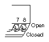
The VME Sync board has a DIP switch bank that is located near the top of the board in back of the front panel status display. See Figure 2-2. For proper operation, the DIP switches should be set according to Figure 2-25 (with switches 1, 2 and 5 in the open position and switches 3, 4, and 6 in the closed position).
| Note: DIP switches 7 and 8 indicate the board address number. Table 2-27 describes the available settings. |
 | Caution: If the system has multiple VME Sync boards, ensure that they each have a different board address number. |
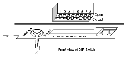
Table 2-24. Settings for Board Address Number 0
Position of Switches 7 and 8 | Corresponding Board Number |
|---|---|
(7) Closed, (8) closed–default setting | 0 (first VME Sync board) |
See Figure 2-26 |
|
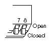
Table 2-25. Settings for Board Address Number 1
Position of Switches 7 and 8 | Corresponding Board Number |
|---|---|
(7) Closed, (8) open | 1 (second VME Sync board) |
See Figure 2-27 |
|
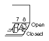
Table 2-26. Settings for Board Address Number 2
Position of Switches 7 and 8 | Corresponding Board Number |
|---|---|
(7) Open, (8) closed | 2 (third VME Sync board) |
See Figure 2-28 |
|
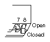
Table 2-27. Settings for Board Address Number 3
Position of Switches 7 and 8 | Corresponding Board Number |
|---|---|
(7) Open, (8) open | 3 (fourth VME Sync board) |
See Figure 2-29 |
|
The VME Sync board comes standard with RS-232 PROMs installed in all four channels. See Figure 2-30. If this is the desired configuration, go to Section 2.4, "Installing the VME Sync Board," to continue installation.
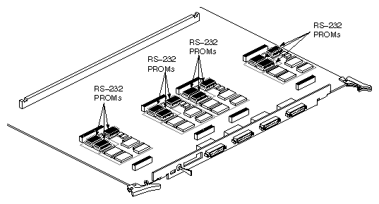
If you need to change the ports to either X.21 or V.35 daughter boards, remove the RS-232 PROM and install the LIMs as follows.
| Caution: Remember, you cannot intermix different interface types on the same board. For example, you cannot have both RS-232 and X.21 LIMs on the same board.In addition, be sure the X.21 or V.35 daughter boards are jumpered according to Figure 2-31 and Figure 2-32. |
Place the VME Sync board and LIM on an antistatic surface.
Use a chip puller to remove the RS-232 PROMs (see Figure 2-30).
Note: Discard the PROMs when you are finished. If you are installing a V.35 LIM, remove the jumpers from jumper blocks 39, 44, 47, and 52. See Figure 2-2 for the location of these jumpers.
If you are installing an X.21 LIM, remove the jumpers from jumper blocks 39, 44, 47, and 52, and then install them on jumper blocks 41, 42, 49, and 50. See Figure 2-2 for the location of these jumpers.
Install the required LIMs component side down in the VME Sync board. See Figure 2-33.
Caution: Be sure to install the LIM in the proper orientation. The VME Sync board and LIM can be damaged if not properly installed.
The VME Sync board is now ready to be installed into the chassis.
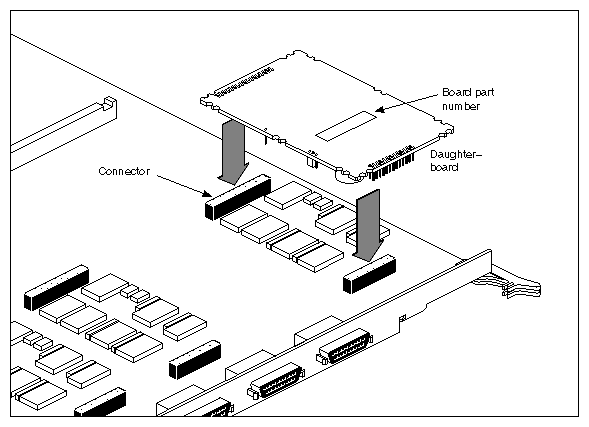
| Note: The X.21 and V.35 daughter boards or line interface modules (LIMs) are physically similar. The only way to differentiate between the two boards is by the part number. See Figure 2-33 for the location of the number. The X.21 daughter board part number is 25190 and the V.35 daughter board part number is 25188. |
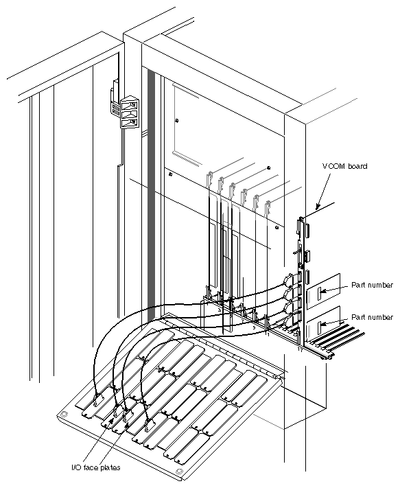
See Figure 2-34 and follow these instructions to install the VME Sync board into a CHALLENGE L (deskside) and XL (rackmount) system.
| Caution: The components are extremely sensitive to ESD (electrostatic discharge). Use proper antistatic procedures while handling all components. |
Prior to your arrival, have the customer back the system up. Afterwards, power off the system using a command such as the following:
shutdown -y -g0
Remove all cables from the I/O door, then open up the door.
Select the appropriate board number address for the VME Sync board, using the on-board DIP switches. See Table 2-27 in Section 2.2.2, "DIP Switch," for more information.
Caution: If you are installing more than one VME Sync board, ensure that each board is assigned a different board number address. See Table 2-27. Note: If you are installing only one board, the VME Sync board should already be correctly configured as board number 0. Depending on the number of available VME slots, a system can support up to four VME Sync boards. Pick an available VME board slot (refer to Table 2-28). When installing VME boards, use the leftmost available slot first and continue installing boards to the right without skipping any slots. This sequence is required since the backplane loops the signals from the left slot to the next slot to the right. Any skipped or open slot interrupts the signal flow to subsequent slots.
Caution: Even if you are using a VME slot located farthest to left, it is a good idea to check the backplane for possible jumpers from a previous installation. If backplane jumpers for this slot are installed, remove them. Note: If you need to skip a VME slot, remember to install backplane jumpers in the appropriate location. See Section 2.5, "Jumpering a Skipped VME Slot," for more details. Table 2-28. VME Slot Positions for CHALLENGE Systems
System Chassis
VME Slot Positions
CHALLENGE L (deskside)
7, 8, 9, 10, and 11
CHALLENGE XL (rackmount)
Cardcage 1 (N/A)
Cardcage 2 (17 through 21)
Cardcage 3(All VME–1 through 21)Install the board into the VME slot. You should hear and feel the board snap into the board ejectors and backplane connectors. The board is now seated in the backplane.
Resecure the board lock bars across the top and bottom of the boards in the cardcage as applicable.
Next, remove a spare I/O plate from the I/O panel for each channel on the board (up to four per board).
Caution: If you have a CHALLENGE L (deskside) system, do not select an I/O plate that is directly in front of the VME Sync or CPU board. Use a blank I/O plate that is either to the right or left of the VME Sync or CPU board. The VME Sync board connectors on the I/O plate are particularly tall and wide and could butt against the connector shells on the VME Sync or CPU board. This would also prevent the I/O door from fully closing. Reattach any I/O cables that have been removed.
With the I/O door still open, power on the system and watch the LEDs on the front panel of the VCOM board(s).
All eight LEDs should flash simultaneously on power-on.
As the VME Sync board cycles through the internal power-on tests, the board LEDs should turn off one-by-one, until only one LED (0, the bottom one) remains flashing. LED 0 provides the heartbeat for the VME Sync and should continue to pulse on and off to indicate normal board operation.
Close the I/O door. See Caution in step 7, if there are any door closing problems.
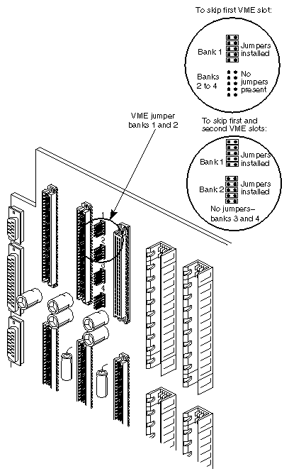
VME boards should be installed left to right, starting with the first available slot on the left. However, skipping a slot is occasionally required to fit oversized VME boards or improve air flow. A slot can be skipped if jumper blocks are placed on the appropriate VME jumper block pins (or headers) located on the rear of the backplane (see Figure 2-35).
| Note: If you install the VME boards in order (from left to right) without skipping, starting with the VME slot farthest to the left, then no jumpering is required. |
The general guideline is to insert jumpers into the jumper banks corresponding to the VME slot number that you are skipping. For example, if you are skipping the first VME slot, you need to insert jumpers into jumper bank 1. See the following additional examples:
If you are skipping the first VME slot (for example, slot 7 in a CHALLENGE L system) to use the next VME slot, you must place five jumpers in the jumper bank, designated as slot 1 (see Figure 2-35).
If you are skipping the first two VME slots and wish to use the third VME slot, you must place jumpers in jumper banks 1 and 2.
If you wish to skip over VME slots, for example, from the first VME slot to the third VME slot, you must place jumpers in bank 2.
Follow these instructions to install and reconfigure the VME Synch board software:
| Note: The VME Sync board requires IRIX version 5.2 for proper support. |
Power-on the system, open up a shell, and become superuser.
Insert the VME Sync CD-ROM and use inst to install the software. For example,
inst -f /CDROM/dist/vsc
Rebuild the kernel by entering the following command at the shell prompt as superuser:
autoconfig -v
This command announces the presence or absence of all optional boards in the system as follows:
exprobe spaced vc adapter n
vc, adapter n exprobe space
The variable n indicates the VMEbus or adapter number.
Reboot and reconfigure the system.
After powering on the system and receiving the system shell prompt, type hinv. You should get a display similar to the following:
VME Synchronous Communications board 0 VME bus: adapter 0 |
The hinv command does not recognize the VME Sync board(s) until the driver from the VME Sync software has been installed and configured into the kernel.