This document describes the procedures used to upgrade an existing Silicon Graphics® Indigo2™ or CHALLENGE™ M system to a POWER Indigo2™ or POWER CHALLENGE™ M system.
 | Caution: This upgrade requires a 64-bit operating system such as IRIX 6.0.1 or later. Part of the upgrade process includes installing a new version of IRIX. |
The POWER Indigo2 and POWER CHALLENGE M systems feature an R8000 CPU module that contains a 75-MHz, 64-bit R8000 RISC chipset. This chipset provides fully separate floating point (FP) and integer units with supporting logic. These POWER systems also contain the IP26 system base board, which has been designed to work with the R8000 CPU module.
The R8000 CPU module has the following major functional elements:
advanced superscalar architecture that supports four instructions per cycle with peak performances of 300 MFLOPs and 300 MIPs
optimized floating point performance with a separate floating point (FP) chip, two FP units, and large load/store data queues
true 64-bit microprocessor with 64-bit integer operations, floating-point operations, and registers
on-chip memory management unit (MMU)
primary 16 KB instruction and 16 KB data caches
a global, 2-MB, 4-way set-associative cache
The POWER Indigo2 and POWER CHALLENGE M systems consume almost exactly as much power and dissipate almost exactly as much heat as the Indigo2 and CHALLENGE M systems. There are no additional site requirements for power and no additional site requirements for cooling.
All other environmental specifications, including humidity, altitude, temperature, and vibration are also unchanged.
The R8000 requires the 64-bit IRIX 6.0.1 (or later) operating system. This is installed as part of the upgrade.
The new power supply (Rev S or later) is mechanically identical to previous revisions. However, the new power supply provides slightly higher nominal 3.3-volt power
(3.45 volts). The increase is required for the R8000 processor as well as for the 200-MHz R4400, the 133-MHz R4600, and future graphics upgrades.
The layout of components on the IP26 system base board is largely unchanged from the IP22. The most significant update is a new memory controller (MC) chip that uses error correcting code (ECC) and provides increased memory (SIMM) capacity. See Section 1.6, "Maximum Memory (SIMM) Configurations," for information on memory capacity.
There are five standoffs on the IP26 board to elevate the R8000 CPU module. Four of these are 40 mm long and one is 18 mm long. The standoffs are 6 mm x M3 and are attached to the IP26 from the bottom with 6 mm x M3 hex nuts. Figure 1-1 shows the locations and sizes of the standoffs.
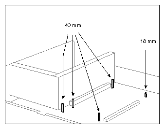
Figure 1-2 shows the component layout of the R8000 CPU board. The R8000 IU and FPU chips are concealed by a heat sink.
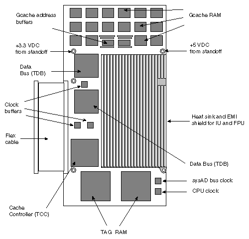
Figure 1-3 provides a logic diagram for both the R8000 CPU module and the IP26 base board. The flex cable noted in Figure 1-2 is the same as the "CPU Module to Base Board Connector" in Figure 1-3.
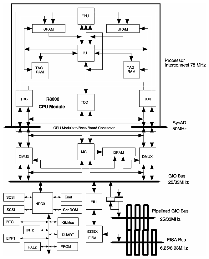
The R8000 has a separate floating point unit (FPU) and integer unit (IU). This is different from the single-chip R4400 processor.
The major advantage of the two-chip implementation of the R8000 is that the main processor (the IU) is no longer tied up performing both integer and floating point operations. Floating point tasks are now executed by a separate FPU in the R8000. The IU and FPU also have dedicated support busing and logic so that their operations can take place simultaneously for maximized CPU board throughput: 300 MFLOPs compared to
40 MFLOPs in the R4400.
 | Note: The R8000 has two dedicated load and store data buses, while single-chip processors such the R4000 have only one load and store data bus. |
Other differences between the R8000 and R4400 systems are highlighted in Table 1-1.
The major internal bus of the R8000 chipset is the 80-bit, 75-MHz Tbus, which connects the IU, FPU, and the cache controller. Ownership of the Tbus changes depending on the operation being performed.
Table 1-1. Differences Between IP22-Based Systems and IP26-Based Systems
Features | IP22 and R4000/R4400 | IP26 and R8000 |
|---|---|---|
Primary cache | R4000: 8 KB instruction, 8 KB data | 16 KB instruction, 16 KB data |
L2 Cache | 1 MB | 2 MB, 4-way associative |
Maximum Memory | 384 MB | 640 MB |
Processor Speed | 100 MHz/150 MHz/200 MHz | 75 MHz |
Issue Rate | 1 per clock | up to 4 per clock |
Peak MFLOPs | ~ 40 | 300 |
Memory References per Clock | 1 | 2 |
Data Path to Memory | 64 bits @ 50 MHz | 128 bits @ 75 MHz |
Kernel Operation Modes | 32 bits | 64 bits |
User Operation Modes | 32 bits | 32 or 64 bits |
The R8000 integer unit (IU) provides a memory management unit (MMU) that uses an on-chip translation lookaside buffer (TLB) to translate virtual address to physical addresses.
The TLB is dual-ported and can get two virtual addresses and come up with two real addresses each cycle. The R8000 TLB is larger than previous TLBs used in previous Silicon Graphics systems. The TLB supports 384 entries and is three-way associative.
In addition, two tag RAMs store address information for even and odd data banks of the interleaved 2-MB streaming cache with dedicated bussing logic.
The maximum memory that can be installed in a POWER Indigo2 and POWER
CHALLENGE M system depends upon the density of the SIMMs, as shown in Table 1-2.
Table 1-2. Maximum Memory Configurations for POWER Indigo2/CHALLENGE M
SIMM Density | Maximum Memory |
|---|---|
4 MB | 48 MB |
8 MB | 96 MB |
16 MB | 192 MB |
32 MB | 384 MB |
64 MB | 640 MB[a] |
[a] Only two of the three SIMM banks can be used with 64 MB memory. Any two banks may contain the 64 MB SIMMs, but the remaining bank must have 32 MB or smaller SIMMs. | |
Within each bank (Bank A, Bank B, and Bank C), SIMMs must be of the same density. Also, be aware that SIMMs in Bank C and SIMM slot S7 (the last slot in Bank B) cannot be taller than 1.27" (approximately 32 mm). See Section 2.1.2, "SIMM Height Limitation."