This chapter highlights the features of the IP21 board upgrade and provides a block diagram description and component drawing.
 | Caution: This upgrade requires a 64-bit operating system such as IRIX 6.1 or later. It should be performed only on stable systems that do not have any unresolved hardware or software problems. |
The IP21 board has one or two R8000 chip sets running internally at 75 MHz or 90 MHz. The IP21 is a triple-height, full-depth, Eurocard board that connects to the existing CHALLENGE and Onyx backplanes. The board contains a mixture of surface-mount and through-hole packaged integrated circuits (ICs).
The IP21 board has the following major functional elements:
an advanced superscalar architecture that supports four instructions per cycle with peak performances of 300 MFLOPS and 300 MIPS for the IP21/75 MHz CPU, and 360 MFLOPS and 360 MIPS for the IP21/90 MHz version
optimized floating-point performance with a separate floating-point (FP) chip and integer unit (IU) chip that are supported by large load and store data queues
a true 64-bit microprocessor with 64-bit integer operations, floating-point operations, and registers
an on-IC memory management unit (MMU)
a 40-bit physical address that enables accessing up to 16 GB of physical memory plus memory-mapped I/O resources
an on-IC, 16 KB instruction cache and 16 KB data cache with 128-bit wide secondary cache interface that supports a secondary 4 MB cache
a streaming cache of 4 MB with four-way interleaving
256 KB of EPROM
The IP21 board dissipates almost exactly the same amount of power as the IP19 board. There are no additional power requirements for CHALLENGE and Onyx systems (such as additional power boards and OLSs). Customer-site power and cooling requirements are also unchanged.
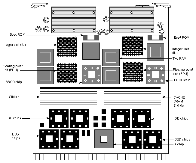
Figure 1-1 shows the physical layout of the IP21 board. Notice that the R8000 CPU consists of two separate ICs: an integer unit and a floating-point unit.
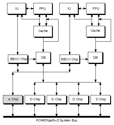
The IP21 is a multiprocessor CPU board that can support one or two R8000 microprocessors. Figure 1-2 provides a functional block diagram of the CPU board. The board logic is divided so that each of the microprocessors has its own dedicated supporting logic. This processor slicing allows each microprocessor to run independently of the other. The only portion of the CPU board circuitry that is shared by the resident microprocessors is the system bus arbitration logic. The system bus is also known as the Everest bus or POWERpath-2™ system bus.
As shown in Figure 1-2, each CPU has its own secondary cache and "blackbird" cache controller (BBCC) chip. Each CPU is also connected to the Ebus through the address path (A) ASIC and four data path (D) ASICs. The D ASICs are the BBD (blackbird data) chips shown in Figure 1-1.
 | Note: "Blackbird" and "TFP" are the in-house code names for the IP21 project. |
Each processor employs a pair of data buffers, the DB ASICS, that load and store to main memory. The DB chips are designed to minimize load latency.
The cache controller implements a duplicate set of secondary cache tags that handle and arbitrate cache requests on the Ebus. The A ASIC services the address requests of all the processors on the CPU board. The D ASIC provides a bit-sliced data path that narrows the 256-bit Ebus data to a 128-bit bus to match the size of the R8000 series interface bus.
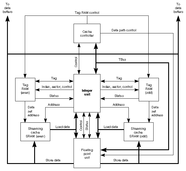
The R8000 has a separate floating-point unit (FPU) and integer unit (IU) (see Figure 1-3). This is different from the single-chip processor R4400 in the IP19 board.
The major advantage of the two-chip implementation of the R8000 is that the main processor (the IU) is no longer tied up performing both integer and floating-point operations. Floating point tasks are now executed by a separate FPU in the R8000. The IU and FPU also have dedicated support busing and logic so that their operations can take place simultaneously for maximized CPU board throughput (see Table 1-1).
| Note: The R8000 has dedicated load and store data buses, while single-chip processors such as the R4000 have only one load and store data bus. |
Other differences between the R8000 and R4400 systems are highlighted in Table 1-1.
The major internal bus of the R8000 chipset is the 80-bit, 75/90 MHz Tbus, which connects the IU, FPU, and the cache controller. Ownership of the Tbus changes depending on the operation being performed.
Table 1-1. Differences Between IP21-Based Systems and IP19-Based Systems
Features | CHALLENGE (IP19) | POWER
CHALLENGE | Onyx (IP19) | POWER Onyx (IP21) |
|---|---|---|---|---|
Maximum CPUs | 36 (XL) | 18 (XL) | 24 (XL) | 12 (XL) |
Maximum IP19/IP21 boards | 9 boards (XL) | 9 boards (XL) | 6 boards (XL) | 6 boards (XL) |
CPUs per Board | 2 or 4 | 1 or 2 | 2 or 4 | 1 or 2 |
L2 Cache | 1 MB, Direct Map | 4 MB, 4-set associative | 1 MB, Direct Map | 4 MB, 4-set associative |
Maximum memory | 16 GB (limited to 2 GB in IRIX 5.2 and earlier) | 16 GB | 16 GB (limited to 2 GB in IRIX 5.2 and earlier) | 16 GB |
Processor speed | 150 MHz | 75 MHz or 90 MHz | 150 MHz | 75 MHz or 90 MHz |
Issue rate | 1 per clock | 4 per clock | 1 per clock | 4 per clock |
Peak MFLOPS | ~50 | 300 (IP21/75) or 360 (IP21/90) | ~50 | 300 (IP21/75) or 360 (IP21/90) |
Memory references per clock | 1 | 2 | 1 | 2 |
Data path to memory, or from the system bus | 64 bits @ 50 MHz | 128 bits @ 75 MHz | 64 bits @ 50 MHz | 128 bits @ 75 MHz |
Kernel operation modes | 32 or 64 bits | 64 bits | 32 or 64 bits | 64 bits |
User operation modes (See note.) | 32 or 64 bits | 32 or 64 bits | 32 or 64 bits | 32 or 64 bits |
| Note: The 64-bit user operations will be supported for the R4400 (IP19) in a future software release. |
The integer unit (IU) in Figure 1-3 provides a memory management unit (MMU) that uses an on-chip translation lookaside buffer (TLB) to translate virtual addresses to physical addresses.
The TLB is dual-ported and can receive two virtual addresses and come up with two real addresses each cycle. The R8000 TLB is larger than TLBs used in earlier Silicon Graphics systems. The TLB supports 384 entries and is three -set associative.
In addition, two tag RAMs store address information for even and odd data banks of the interleaved 4 MB streaming cache with dedicated busing logic (see Figure 1-3).