This chapter provides a block diagram description of the CHALLENGE/Onyx system. A functional overview of the RealityEngine2 (RE2) and VTX graphics board set is also provided.
Figure 4-1 shows a simplified block diagram of the CHALLENGE/Onyx bus and system architecture. Each board that composes the board set, as well as the optional interface modules, VCAM, and SCSI channel configuration boards is described in detail in the following sections.
The base CHALLENGE/Onyx system configuration includes these boards:
an IP19 CPU board
an MC3 memory board
an IO4 system I/O board
Both the Onyx graphics and the CHALLENGE server configurations of the chassis are shipped with a version of the system board set. Additionally, a number of optional (mezzanine) boards may be attached to the IO4 board.
The principal features of the system board set are:
two or four R4400 microprocessors per CPU board
1.2 GB per second, 256-bit bus
48-bit address bus
RealityEngine2/VTX graphics subsystem support
up to two GB of interleaved RAM
dual SCSI-2 channels for each IO4 board
8- and 16-bit SCSI II compatibility
Additional Flat Cable Interface (FCI), VMEbus, and SCSI ports available on optional mezzanine boards
The main set of buses in the CHALLENGE/Onyx system architecture is the Everest address and data buses, Ebus for short. The Ebus replaces the old standard MP bus in the Silicon Graphics POWER Series™ systems such as the Single Tower and POWER Center™ (Predator). The Ebus provides a 256-bit data bus and a 40-bit address bus that can sustain a bandwidth of 1.2 GB per second. This is 20 times greater than the bandwidth of the old MP bus.
 | Note: The Ebus may be referred to as the POWERpath-2 system bus in other documents. |
The 256-bit data bus provides the data transfer capability to support a large number of high-performance RISC CPUs. The 40-bit address bus is also wide enough to support 16 GB of contiguous memory in addition to an 8 GB I/O address space.
The 64-bit Ibus (also known as the HIO bus) is the main internal bus of the I/O subsystem and interfaces to the high-power Ebus through a group of bus adapters. (See Section 4.4.1.1, "Bus Architecture," for more information.) The Ibus has a bandwidth of 320 MB per second that can sufficiently support a graphics subsystem, a VME64 bus, and as many as eight SCSI channels operating simultaneously.
Another major bus in the CHALLENGE/Onyx architecture is the 64-bit VMEbus. The VMEbus interfaces with the Ebus through the VCAM board, which mounts on the IO4. Additional VMEbuses may be added to the CHALLENGE/Onyx rackmount system through an optional card cage.
The VME interface supports all protocols defined in Revision C of the VME specification plus the A64 and D64 modes defined in Revision D. The D64 mode allows DMA bandwidths of up to 60 MB.
The system controller assembly consists of a PCB and LCD screen. The PCB contains a battery-backed microprocessor that communicates directly with the boot-master CPU board through a polled serial line. For a complete discussion on the operation of the System Controller, see the CHALLENGE/Onyx Diagnostic Roadmap, Document No. 108-7045-xxx.
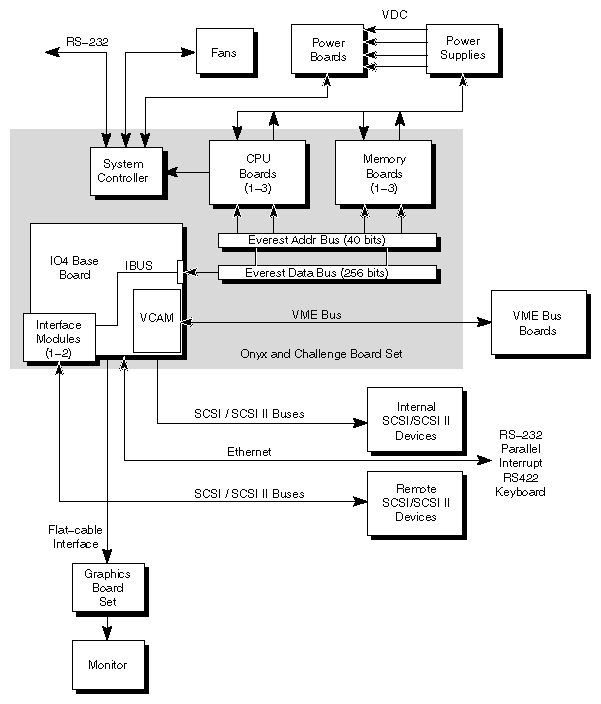
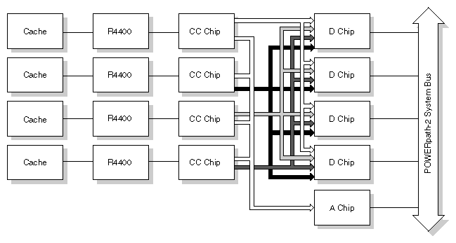
The IP19 is a multiprocessor CPU board that can support two or four R4400 microprocessors. The board logic is divided so that each of the microprocessor has its own dedicated supporting logic. This processor slicing allows each microprocessor to run cache-independent of the others. The only portion of the CPU board circuitry that is shared by the resident microprocessors is the bus arbitration logic. See Figure 4-2 for a functional block diagram illustrating the CPU board.
Here are some of the key features of the MIPS R4400,which is the main processor in the CHALLENGE/Onyx systems:
true 64-bit microprocessor with 64-bit integer and floating-point operations, registers, and virtual addresses
50 MHz external clock frequency and 100-MHz internal clock frequency (at initial product shipment)
on-IC memory management unit (MMU)
5-volt or 3.3-volt power supply
36-bit physical address than can access up to 64 GB of physical memory
64-bit cache-coherent system interface
on-IC 16 KB instruction cache and 16 KB data cache with 128-bit secondary cache interface that can support a secondary cache size of either 1 or 4 MB
64-bit virtual address
As shown in Figure 4-2, each CPU has it own secondary cache and a cache controller, the CC device. Each CPU is also connected to the Ebus through the address path (A) ASIC and four data path (D) ASICs.
The cache controller implements a duplicate set of secondary cache tags that handle and arbitrate cache requests on the Ebus. The CC arbitrates requests by giving read-request operations a higher priority than cache-write requests. Pending bus access requests are then buffered and queued until the current operation is complete.
The A ASIC services the address requests of all the processors on the CPU board. Like the CC, the A ASIC gives higher priority to read requests to minimize the read-wait or read-latency period. It also supports piggyback read requests from different processors, allowing several processors to share the same read requests and response cycles on the bus. This helps optimize overall performance for tightly coupled microprocessing programs. Even though the A ASIC may service up to four processors, each processor still has its own dedicated path to the bus.
The D ASIC provides a bit-sliced data path that narrows the 256-bit Ebus data to a 64-bit bus to match the size of the R4000 series interface bus. Each processor has its own 64-bit path dedicated for transfers to the system bus. Again, there is no contention between processors sharing the same CPU board. The data path between the CC and D ASICs is bidirectional. To minimize read latency, the default direction for this bus is toward the processor.
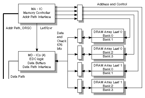
The MC3 memory board is arranged so that its SIMMs are separated into two DRAM array leaves (leaf 0 and leaf 1). Each array leaf has four banks of four SIMMs each. The system supports 16 and 64 MB SIMM sizes and allows a maximum capacity of 2 GB per MC3 board.
| Note: Earlier versions of the MC3 (P/N 030-0245-007 and below) supported a maximum of 1 GB of system memory owing to problems with the MA ASIC. Newer versions of the MC3 (P/N 030-0245-008 and above) will support up to 2 GB of memory. |
Two types of interleaving are supported: on-board interleaving between array leaves of equal memory size on the same board and interleaving between two or more memory boards having the same total memory capacity. Figure 4-3 is a functional block diagram of the MC3 board.
Interleaving, a technique for organizing memory into leaves, increases the sustainable memory bandwidth. For example, using two overlapped memory accesses, operating on two memory leaves, effectively doubles the memory bandwidth attainable without interleaving. (A single memory leaf can start to process a new read request every 200 nanoseconds; the Ebus can deliver a new request every 100 nanoseconds.) Each leaf can independently process a memory request for a processor.
Each memory board supports two-way interleaving, and each leaf can transfer an entire cache block, which is the unit of interleaving. Two memory boards support up to four-way memory interleaving; four memory boards support up to eight-way interleaving.
| Note: If a memory problem occurs, this could seriously affect the interleave factor for the system. For example, if the system is set up for two-way interleaving and a problem occurs with one of the SIMMs, the system could default to one-way interleaving because the memory link is broken. |
The key memory board components are (see Figure 4-3)
one address control ASIC (the MA IC)
four data control ASICs (the MD ICs)
custom SIMMs
The MA ASIC is a gate array that provides the interface between the memory array and the system address lines, or address path. The MA ASIC includes bus arbitration and acknowledge logic, decode logic, and two interleaved DRAM controllers. Each DRAM controller generates multiplexed memory address lines and control lines to control two banks of DRAM SIMMs. In addition, the MA IC generates and receives signals that allow it to control the MD ASICs.
The four MD ASICs provide error detection and correction and data buffering for the transfer of data between the 576-bit-wide memory array and the 264-bit-wide D path, including ECC bits. The MD ASICs perform no action on their own, except notifying the MA ASIC when they detect an error. The four MD ASICs are identical; each drives one quarter of the bus.
The memory array consists of one to eight banks of 144 four-bit-wide DRAMs of either
16 MB or 64 MB. Groups of 36 memory ICs, together with their associated address buffers, are mounted on 200-pin SIMMs. Each SIMM provides 144 bits of data. A complete memory bank consists of four identical SIMMs.
A minimum configuration of 64 MB uses four SIMMs. A maximum configuration uses 32 SIMMs. Normally at least two memory banks are populated. For maximum performance, the two banks must be located on different memory leaves; all memory banks must have the same number of populated leaves. If half the Ebus-rated performance is sufficient, a system can be configured with a single memory bank.
This section details the operation of the IO4 subsystem. The CHALLENGE/Onyx I/O subsystem consists of an IO4 base board and a set of optional I/O mezzanine boards that mount directly onto the IO4 board.
The IO4 board is the heart of the I/O subsystem. The IO4 board supplies the system with a basic set of I/O controllers and system boot and configuration devices. This base set include:
three RS-232 ports
one RS-422 port
one parallel port
one Ethernet controller
a second-level boot EPROM
an NVRAM that stores system configuration information
two Ibus connections
In addition, the IO4 board provides these interfaces:
two Flat Cable Interconnects (FCIs)
two SCSI-2 cable connections
two Ibus connections
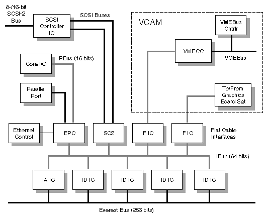
See Figure 4-4 for a functional block diagram of the IO4 board.
Communication with the VME and SCSI buses, the installed graphics boards set(s), and the Ethernet takes place through the Ibus. A set of interface control devices, an I address (IA) and I data (ID), interfaces the Ibus to the Ebus, the main system bus. The ID ASICs latch the data, and the IA ASIC clocks the data from each ID to the Flat Cable Interface (FCI).
Two FCI controllers (or F controllers) handle the data transfers to and from an internal graphics board set (if installed) and any VMEbus boards. The SCSI-2 (S) controller serves as an interface to the various SCSI-2 buses. The Everest peripheral controller (EPC) device manages the data movement to and from the Ethernet, a parallel port, and various types of on-board PROMs and RAM.The EPC communicates with the second-level boot PROM, the system configuration NVRAM, and the timer through the peripheral bus, or Pbus. The Pbus is a 16-bit general-purpose bus that is designed for components using external DMA controllers or PIO.
The S controller is an ASIC that contains two SCSI-2 controller ICs and the logic to interface with the Ibus. The S controller provides two fast and wide 16-bit SCSI-2 controllers that are configurable as either single-ended or differential. See Section 4.4.2.4, "SCSI Channel Adapter Boards," for more information.
The F controller acts as an interface between the Ibus and the Flat Cable Interfaces (FCIs). This device is primarily composed of FIFO registers and sychronizers that provide protocol conversion and buffer transactions in both directions and translate 34-bit I/O addresses into 40-bit system addresses.
Two configurations of the F controller are used on the IO4 board; the difference between them is the instruction set they contain. One version is programmed with a set of instructions designed to communicate with the GFXCC (for graphics), the other version has instructions designed for the VMECC. All communication with the CC ICs is done over the FCI, where the F controller is always the slave.
Both versions of the F controller ASICs have I/O error-detection and handling capabilities. Data errors that occur on either the Ibus or the Ebus are recorded by the F controller and sent to the VMECC or GFXCC (the CC ICs must report the error to the appropriate CPU and log any specific information about the operation in progress). FCI errors are recorded in the error status register. This register provides the status of the first error that occurred, as well as the cause of the most recent FCI reset.
The Everest peripheral controller (EPC) supports the basic peripheral ICs and interfaces required for system boot and operation. The EPC manages the data movement to and from the Ethernet, a parallel port, and various types of on-board PROMs and RAM. The EPC consists of the following components:
a SEEQ EDLC Ethernet controller and buffer
a real-time clock with battery-backed RAM
one MB of EPROM, a small serial EEPROM
a SCSI-channel buffer
a DMA engine
three Zilog 85230 DUARTs
Note: One of the Zilog ICs supports the mouse and keyboard. The other two drive the four serial ports.
Two additional devices are connected to the EPC IC: a Western Digital SCSI-1 interface IC for use with single-ended SCSI devices and static RAM for use as buffer memory. The EPC also supports a parallel port.
Other principal components of the I/O subsystem are mezzanine boards. The mezzanine boards mount directly onto the IO4 base board through a set of standoffs. The available mezzanine boards consist of these types:
a VCAM board
an S mezz board that provides three additional SCSI channels
two versions of the FCI interface board
two SCSI channel adapter boards
The mezzanine boards provide the IO4 board with a variety of additional bus interfaces and/or serial ports. The mezzanine boards mount directly to the IO4 board. Brief descriptions of the available mezzanine boards follow.
The VCAM board comes standard with the system and mounts on the rear of the IO4 base board through a set of standoffs. The VCAM board provides the interface between the Ebus and the VMEbus and manages the signal level conversion between the two buses. The VCAM also provides a pass-through connection that ties the graphics subsystem to the Ebus.
The VCAM can operate as either a master or a slave. It supports DMA-to-memory transactions on the Ebus and programmed I/O operations from the system bus to addresses on the VMEbus. In addition, the VCAM provides virtual address translation capability and a DMA engine that increases the performance of non-DMA VME boards.
The SCSI (S mezz) board duplicates the SC2 IC and SCSI control logic found on the IO4 base board and provides three additional SCSI channels. Two of the channels are differential only; the third is configurable as single-ended or differential. The IO4 base board can house up to two S mezz boards and provide up to eight SCSI channels. In this maximum SCSI channel configuration, four channels are reserved for differential operation only. The other four channels can be configured as either single-ended or differential. This board secures to the IO4 board through standoffs.
The F mezzanine (F mezz) boards duplicate the F controller (see Section 4.4.1.3, "F Controller ASIC") and control logic found on the IO4 board. The two FCI boards are designated F mezz and F mezz (short). The only differences are that the F mezz board is slightly longer and has an additional connector. This connector allows it to pick up the FCI channel normally covered by the VCAM. The long F mezz board is used only in systems having multiple IO4 boards and on those boards that do not have the VCAM mounted. The short version of the F mezz is designed to mount on the IO4 board along with the VCAM. The long F mezz provides two additional interfaces to the FCI. The short version has one less interface.
The CHALLENGE/Onyx systems are powered through an offline switcher (OLS) and a set of specialized power boards. The following sections describe these components in detail.
The deskside chassis supports a 1900-watt OLS that accepts 110 or 220 VAC without jumper modifications. The OLS converts the input voltage to 48 VDC and distributes the regulated voltage to a set of backplane power boards. The power boards then take the 48 VDC and converts it to 5 and 12 VDC.
The rackmount chassis supports a maximum of three 1900-watt OLSs to provide power for the system's multiple card cage and backplane architecture.
In the rackmount configuration, the OLSs convert the 220 or 400 VAC input to 48 VDC at 37 amps and distribute the regulated voltage to the chassis midplane. Additional power boards supply the DC voltages required by the Everest and VMEbuses. The on-board regulators and power boards allow board-level voltages to be generated for only the populated card cage slots.
Power boards are DC-to-DC converters that take the 48 volts from the offline switcher and step it down to levels appropriate for the buses, circuit boards, and SCSI drives. The power boards connect to the CHALLENGE/Onyx backplane. Three types of power boards are used in the CHALLENGE/Onyx deskside system:
The System Controller board supplies +1.5 VDC at 30 amps for use by the Ebus. This board also provides power for the microprocessor in the System Controller.
The 505 power board generates +5 VDC at 80 amps for use by the boards.
The 512 power board generates +5 VDC at 40 amps and +12 VDC at 17 amps for the VMEbus.
Unless otherwise indicated, the following sections apply to both the RE2 and the VTX configurations.
The RealityEngine2 (RE2) and VTX are the graphics boards sets in the Onyx deskside and rackmount systems. The RE2 and VTX graphics subsystems comprise three board types: the Geometry Engine (GE10), the Display Generator (DG2), and the Raster Memory (RM4).
The principal features of the RealityEngine2 and VTX graphics board sets are
greater texel storage capacity (4 MB versus 256 KB in PowerVision™)
greater texturing and antialiasing capabilities
more color and greater depth and spatial resolution
RGB and simultaneous low-resolution composite video out
supports most video standards, such as PAL and NTSC
built-in genlocking
greater z-buffering capability (32 bits versus 24 bits in PowerVision)
supports full-scene antialiasing (1K x 1K)
higher pixel processing power
separate 12-bit color maps for multiple windows
The RE2 provides greater performance than the RealityEngine graphics as a result of enhanced GE processing hardware and the expanded bandwidth of the Everest bus. The VTX (a 5-span-only configuration) is a cost-reduced version of the RE2.
Major similarities between these board sets include the following:
All three graphic subsystems use the DG2 (Display Generator) board.
All three graphic subsystems use the RM4 (Raster Memory) board.
For a list of differences among these subsystems, see Table 4-1.
Table 4-1. Differences Among VTX, RealityEngine2, and RealityEngine Subsystems
Feature | RealityEngine | ||
|---|---|---|---|
Number of RM4 boards and number of spans supported | 1 RM4 board (5 span only) | 1, 2, or 4 RM4 boards (5, 10, or 20 span) | 1, 2, or 4 RM4 boards (5, 10, or 20 span) |
Monitor size and maximum resolution supported | 19-inch (1280 x 1024 resolution) | 21-inch (1600 x 1200 resolution) | 21-inch (1600 x1200 resolution) |
Geometry Engine board used and number of GE processors | GE10V with 6 GE processors | GE10 with 12 GE processors | GE8 with 8 GE processors |
No | Yes | Yes | |
RM4T board required | No | No | Yes |
Frontplane used | DI4 | DI1 for Onyx rackmount and DI3 for Onyx deskside | DI1, DI2, DI3, depending on system |
Supported systems | Onyx deskside and rackmount | Onyx deskside and rackmount | POWER Series systems including — POWER Center (Predator) — SkyWriter — Single Tower — Crimson |
Number of heads or pipes supported | 1 only | 1 on Onyx deskside and 1 to 3 on Onyx rackmount | 1 on all supported systems. SkyWriter supports up to two heads. |
| Note: The RealityEngine uses an RM4T (Raster Memory terminator) board to terminate the triangle bus. The triangle bus is terminated through the backplane for the RE2 and VTX graphics. |
The primary board in the subsystem is the GE10. The GE10 interfaces with the host system through a Flat Cable Interface (FCI) connection that ties to the VCAM mezz board on the IO4 base board (see Figure 4-5). The FCI connection is embedded in the backplane of the system.
An F controller (see Section 4.4.1.3, "F Controller ASIC") on the IO4 base board provides a Flat Cable Interface to the VCAM board. Graphics data routes from the VCAM to the backplane to the GE10.
The GE10 communicates with the RM4(s) over the triangle bus and with the DG2 board over the Video Control (VC) bus. The Video Control bus provides access to the color maps, window display modes, and cursor control modes. Communication between the RM4(s) and the DG2 board is over the video bus. Figure 4-5 shows a block diagram of the RealityEngine2 and VTX board set.
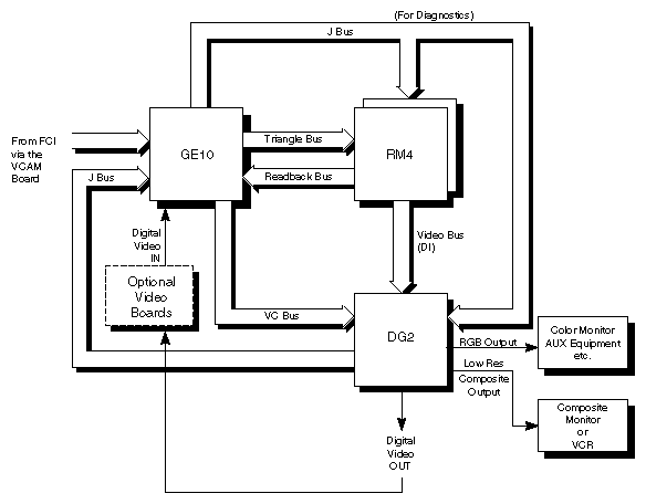
The RealityEngine2 and VTX board sets use application-specific integrated circuits (ASICs) and parallel processing to reduce the amount of required hardware. This reduction can be seen when the RealityEngine2 and VTX are compared to their predecessor, PowerVision. The RealityEngine2 and VTX have three standard boards; PowerVision requires a minimum of four boards.
| Note: The GE10 performs the functions of the GE6 and GM3 (geometry manager) board of the PowerVision system. |
The Geometry Engine (GE10) board processes graphics library (GL) commands and data from the system CPU board and is the first stage of the graphics pipeline. Figure 4-6 shows a block diagram of the GE10.
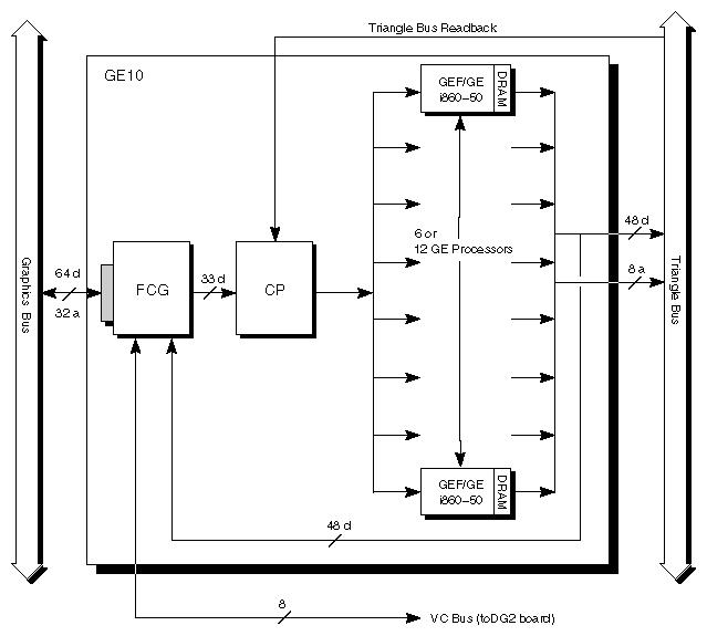
The major components on the GE10 are the Flat Cable Interface–to- graphics (FCG) ASIC, the command processor (CP), and the geometry engine (GE) processors.
The FCG ASIC interfaces data from the Flat Cable Interface through the VCAM to the graphics pipeline and transmits the data to the CP. The CP acts as the central distributing point for the data and instructions and reorders the input stream for efficient processing. The CP distributes data to the GE processors over a 32-bit bus.
The GE10 (RE2 version) has 12 GE processors. The GE10V (VTX version) has six GE processors.The GE processors consist of a floating-point microprocessor, the Intel™ i860XP, a 64-bit-wide DRAM, which stores both code and instructions, and the Geometry Engine FIFO (GEF) ASIC (see Figure 4-7). The Intel microprocessor can perform 100 million floating-point operations per second (MFLOPS).
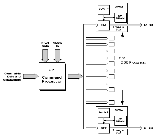
The GE10 ties into the display generator subsystem (the DG2) board through the video control bus. This bus allows access to color maps, window display modes, and cursor control as well as video format and timing control.
The Raster Memory (RM4) boards scan and convert triangle data from the triangle bus into pixel data. The RM4 then organizes the data into a series of spans (vertical strips of pixels) and transfers it to the frame buffer. The frame buffer is a rectangular array of image memory processors.The graphics subsystem displays images by projecting continuous spans onto the screen. Following the transfer to the frame buffer, the RM4 hands off control of the graphics subsystem to the display generator (DG2). The RM4 board is shown in Figure 4-8.
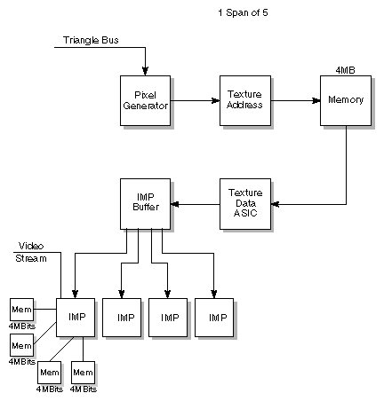
The RE2 board set can have up to four RM4 boards per pipeline. The cost-reduced VTX supports one RM4 board. As more RM4 boards are added, the spans are interleaved, providing higher resolution and display quality.
| Note: A 10-span system has 10 pixel generators, 160 image engines and increased memory. A 20-span system has 20 pixel generators, 320 image engines, and even greater memory. |
To differentiate the boards, the RM4s receive a 2-bit identity field from the video bus front plane, the DI1. This field identifies which of four addresses a board occupies.
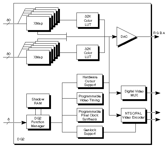
The DG2 board receives digital frame buffer pixel data from the RM4 board over the video bus. The DG2 then processes the pixel data through digital-to-analog converters (DACs) to generate an analog pixel stream for display. The principal components of the DG2 board are the XMAP ASICs, the function manager ASIC, and an NTSC/PAL encoder (see Figure 4-9 for a functional block diagram of the DG2 board).
The ten XMAP ASICs on the DG2 board receive the serial stream of digital video data from the video control (VC) bus. The ASICs reorder data from the frame buffer to provide a left-to-right scan line display. The XMAPs also handle the lookup of the color-mapped pixels and generate the proper RGB color for each pixel.
The function manager ASIC controls these display and video control tasks for the DG2 board:
cursor display
video timing
pixel clock
genlocking
SCSI front-loading devices (FLDs) require no additional cabling at installation; however, each device should be checked to ensure that it has a valid ID select number. The location of the ID select switch varies according to the make of drive being installed.
The internal SCSI buses terminate on the SCSI backplane, which is part of the drive bulkhead assembly (see Chapter 2, "Chassis Tour," for more information). If remote SCSI drives are to be connected to the internal SCSI bus, remove the cable from the SCSI channel the cable, remove the bus terminator, and attach a SCSI cable of the correct length between the remote drives and the CHALLENGE/Onyx system I/O panel. Ensure that the bus is correctly terminated at the last remote device.
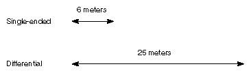
| Note: The maximum allowable length for single-ended SCSI cabling is 19.6 feet (6 meters), and the maximum allowable length for differential SCSI cabling is 81 feet (25 meters). |
These guidelines also apply to systems having additional SCSI channels owing to the installation of one of the optional mezzanine cards.
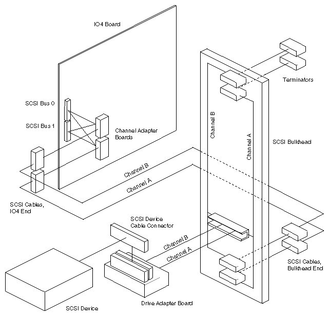
The CHALLENGE/Onyx products support many types of SCSI protocols, resulting in a wide variety of SCSI channel configurations. This document introduces the supported SCSI protocols for CHALLENGE/Onyx products, defines the components in a SCSI channel, and explains how to configure and label a SCSI channel.
SCSI devices continue to evolve with higher bus bandwidths, faster data transfer rates, and channels with longer cables and more devices.
A protocol establishes a SCSI bus's bandwidth, type, and data transfer rate. These factors depend on one another. For example, a 16-bit SCSI peripheral typically transfers more data at a faster rate than an 8-bit SCSI peripheral.
An 8-bit bus provides up to eight SCSI IDs; a 16-bit bus provides up to 16 SCSI IDs. Because a SCSI bus controller uses the first SCSI ID (ID #0), 8-bit buses use seven SCSI IDs for devices and 16-bit buses use 15 SCSI IDs.
A SCSI bus type is either single-ended or differential. Differential buses use circuitry to obtain higher signal levels in a bus than normally possible with single-ended buses, as shown in Figure 4-10. Higher signal levels support longer cable lengths and more devices on a bus. Single-ended and differential SCSI peripherals use different integrated circuitry and cannot be mixed on a bus.
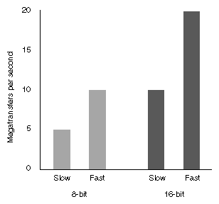
Data transfer rates are either slow or fast, measured in megatransfers per second. Megatransfers are the millions of operations per bus cycle. An operation is either 8- or 16-bit in size. Megatransfers are based on a bus's burst data rate. Data transfer rates depend on the bus bandwidth. See Figure 4-11.
The system controller negotiates independently with the devices on a bus to establish the acceptable transfer rate of each device, allowing a mix of fast and slow devices on the same bus.
These guidelines reflect the dependencies between SCSI bus bandwidths, types, and data transfer rates. Follow these guidelines to minimize inconsistent or inoperable SCSI buses:
Install 8-bit and 16-bit devices on separate buses.
Install single-ended and differential devices on separate buses.
When calculating SCSI bus length, include all cable-length inside devices, components, and chassis.
A SCSI channel can include a mix of these components:
a board that generates the signal
all cabling from the start to the end of a channel
all converters and adapters in the cable path
all SCSI devices connected to the channel
a terminating device at the end of the channel
See Section 4.9.1, "SCSI Channel Component and Descriptions" for a description of the typical components in an Everest SCSI bus and Figure 4-20 for an overview of the default chassis SCSI implementations for the deskside chassis.
This section describes the various SCSI channel components.
| Note: The SCSI component drawings are not to scale. |
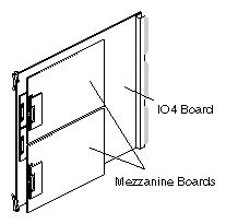
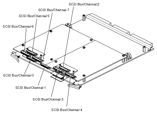
An IO4 board (see Figure 4-12) provides SCSI bus signals for up to eight SCSI buses. SCSI buses 0 and 1 are available directly on the IO4 board. Buses 2 through 4 require a mezzanine board attached to the lower mezzanine connector on the IO4 board, and buses 5 through 7 require a second mezzanine board attached to the upper mezzanine connector.
IO4 boards support all SCSI protocols and use an adapter board to select the desired protocol for each bus. Several IO4 boards may reside in a system.
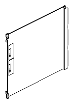
A SCSI mezzanine board (see Figure 4-13) attaches to an IO4 board, up to two mezzanine boards for each IO4 board. Each SCSI mezzanine board supports three SCSI buses.On the inner connectors, two buses use differential protocol only, and on the outer connector, the bus is selectable as either single-ended or differential by using a Channel adapter board.
The first mezzanine board provides SCSI buses 2 through 4, with bus 2 on the outer center connector. The second mezzanine board provides SCSI buses 5 through 7, with bus 5 on the outer center connector.
A channel adapter board (see Figure 4-14) adapts a SCSI bus for either single-ended or differential protocol. Channel adapter boards attach directly to an IO4 board or to the outer connector on a SCSI mezzanine board.

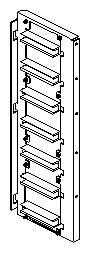
A SCSI bulkhead (see Figure 4-15) supplies a blind-pluggable receptacle to each SCSI device bay in a SCSI box. Each receptacle provides up to two SCSI channels, selectable using a drive adapter board.The bulkhead also provides connectors at the end of the channels for termination.Several different SCSI bulkheads exist based on the chassis involved.
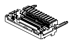
A 50-pin drive adapter board (see Figure 4-16) selects one of the two possible SCSI channels delivered to each drive bay. A drive adapter board resides on a drive sled and provides a blind-pluggable connection between a SCSI device and the SCSI bulkhead. The 50-pin adapter board is used for drives that use a 50-pin cable, which are typically single-ended devices.
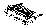
A 68-pin drive adapter board (see Figure 4-17) selects one of the two possible SCSI channels delivered to each drive bay. A drive adapter board resides on a drive sled and provides a blind-pluggable connection between a SCSI device and the SCSI bulkhead. The 68-pin adapter board is used for drives that use a 68-pin cable, which are typically differential devices.
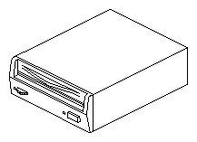
A SCSI device (see Figure 4-18) is a media retrieval mechanism that uses the SCSI interface.
A SCSI terminator (see Figure 4-19) resides at the end of a SCSI channel and terminates the signals. A SCSI channel will not work unless the signals are properly terminated.
An IO4 board can have up to eight SCSI bus interfaces or channels (see Figure 4-21). Compare this with the IO3, the predecessor to the IO4, which has only two channels (or SCSI bus interfaces). In addition, the new, wider SCSI pin connector on the chassis now has 68 pins that enable connectivity with up to 15 devices per channel.
Due to this expanded connectivity, the IRIX and PROM monitor drive-addressing scheme has been modified to accommodate the increased number of drives and channels.
The previous PROM drive addressing format remains basically in place, for example, dksc(a,b,c), where a represents the SCSI bus number, b refers to the drive number, and c refers to the drive's partition number. The dksc designation is the monitor's name for SCSI.
| Note: The PROM can address only the master IO4 board in a system. In a deskside system, the master IO4 resides in either slot 3 (Onyx) or slot 5 (CHALLENGE). In a rackmount system, the master IO4 resides in slot 15. If you need to address a drive connected to another IO4 board, you must do so under IRIX. |
Under IRIX, the addressing scheme has changed as shown in the following new format, /dev/dsk/dksSSSdDsP, where /dev/dsk references the IRIX file directory of the drives and dks designates SCSI. The SSS designator represents the slot number of the IO4 board and/or the SCSI bus number (see Note below), dD refers to the drive number, and sP refers to the drive's partition number.
| Note: If you are addressing a drive on the master IO4 board system, you need to specify only the applicable SCSI bus number. If you are addressing a drive on another IO4 board, you must specify both the slot number of the board and the applicable SCSI bus number. |
For example, if you are addressing a drive connected to an IO4 board in slot 4 and SCSI bus number 5 (on a deskside system), the SSS number would be 45.
With the earlier IO3 boards, the software required only single digits to differentiate drives; however, with the IO4 and new version of the software, the SCSI bus or SSS number can contain up to three digits. If SSS is a two- or three-digit number, the first one or two digits identify the IO4 board, by the Ebus slot number. The final digit identifies which of the eight possible SCSI buses (0 through 7) on the IO4 board is used. See Figure 4-21 to see how the buses are physically laid out on the IO4 board.
The software drive identification number uses the same form as in the addressing scheme described earlier. Insert the IO4 board slot number and/or the SCSI bus number, followed by the drive number and partition number as required.
Assume that you want to address partition 0 on SCSI drive (number 6). This drive connects to SCSI bus number 6. You can also assume that the IO4 resides in slot number 15 in a rackmount system.
The PROM drive address is dksc(6,6,0).
Assume that you want to address partition 0 on SCSI drive (number 6). This drive connects to SCSI bus number 6. You can also assume that the IO4 resides in slot number 14.
The IRIX drive address is /dev/dsk/dks146d6s0.