This appendix summarizes hardware specifications for the HD I/O Board and its cable, in these sections:
Figure A-1 shows the two multiheaded cables included with the board; each has four 50-pin connectors for link A input, link B input, link A output, and link B output. The 50-pin connectors differ for each type of cable, following the Panasonic and Philips 50-pin video equipment interface standard.

Table A-1 summarizes the Panasonic (HD-D5) pinout for the cable's 50-pin connector.
Table A-1. Panasonic 50-Pin Connector Pinout (HD-D5)
Pin | Signal | Pin | Signal | Pin | Signal |
|---|---|---|---|---|---|
1 | CLK+ |
|
| 34 | CLK- |
Table A-2 summarizes the Philips (Spirit DataCine) pinout for the cable's 50-pin connector.
| Note: An early version of the Phillips 50-pin connector (SGI PN 018-0802-001) has a known wiring error. If you have this connector, contact your sales or service representative for a replacement connector |
Table A-2. Philips 50-Pin Connector Pinout (Spirit DataCine)
Pin | Signal | Pin | Signal | Pin | Signal |
|---|---|---|---|---|---|
1 | CLK+ |
|
| 34 | CLK- |
Table A-3 summarizes the use of the LINK A connector for 4:2:2 mode. The LINK A connector carries 10-bit wide UVY information.
Table A-4 summarizes usage for 10-bit RGBA.
Table A-4. LINK A and LINK B Usage in RGBA Mode
Sample | LINK A | LINK B |
|---|---|---|
0 | B0 G0 | B1 A0 |
1 | R0 G1 | R1 A1 |
2 | B2 G2 | B3 A2 |
3 | R2 G3 | R3 A3 |
Table A-5 summarizes the use of LINK A and LINK B connectors for 4:4:4:4 mode. The LINK A connector carries a 4:2:2 sampled portion of 10-bit wide UVY; the LINK B connector carries the remaining 10-bit UV samples and 10-bit alpha. Usage is similar for 10-bit RGBA.
Table A-5. LINK A and LINK B Usage in 4:4:4:4 Mode
Sample | LINK A | LINK B |
|---|---|---|
0 | Cr0 Y0 | Cr1 A0 |
1 | Cb0 Y1 | Cb1 A1 |
2 | Cr2 Y2 | Cr3 A2 |
3 | Cb2 Y3 | Cb3 A3 |
The General Purpose Interface (GPI) port provides two channels of input and output trigger signal pairs on one connector. This section consists of the following subsections:
Figure A-2 shows the GPI connector on the HD I/O panel.

Figure A-3 shows the pinouts for the GPI connector.
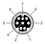
Table A-6 defines each of the pins in Figure A-3.
Pin | Use | For Video Pipe | CCT/CCR |
|---|---|---|---|
8 | In transmit + | In | CCT + |
4 | In transmit - | In | CCT - |
5 | Out transmit + | Out | CCT + |
2 | Out transmit - | Out | CCT - |
6 | In receive + | In | CCR + |
7 | In receive - | In | CCR - |
3 | Out receive + | Out | CCR + |
1 | Out receive - | Out | CCR - |
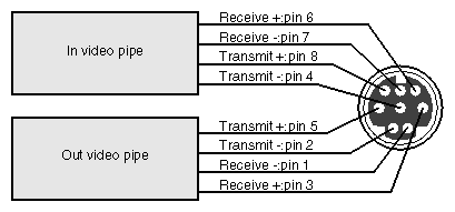
Figure A-4 diagrams the relationship between the HD I/O Board's video pipes and the GPI pins.
GPI contact closure transmit (CCT) outputs use an optically coupled solid-state relay (SSR) to provide a means of electrical isolation for destination equipment.
Table A-7 and Figure A-5 show electrical specifications for the GPI transmitter.
Table A-7. GPI Transmitter Electrical Specifications
Parameter | Value |
|---|---|
On resistance | 10 ohms typical, 15 ohms maximum |
Off resistance | 5000 G ohms |
Current limit | 360 mA typical, 460 mA maximum |
Output capacitance | 60 pF |
Continuous DC load current | 180 mA |
Output power dissipation | 600 mW |
Isolation voltage | 3750 V rms |

The GPI transmitter can be interfaced to the destination equipment by tying the CCT- terminal to GND and using the CCT+ terminal as a current sink. The input device of the destination equipment can consist of a logic device with active pullup, an optoisolator LED with series-limiting resistor, or relay primary with series-limiting resistor.
The GPI transmitter's logic sense can be swapped (inverted) by tying the CCT+ terminal to the logic power supply (VCC) of the destination equipment and using the CCT- terminal to drive the input of the receiving device.
GPI receive (CCR) inputs use an optical isolator device to provide a means of electrical isolation from source equipment. The device consists of a bidirectional input LED optically coupled to a bipolar transistor. A voltage pulse applied across the CCR+/- pins causes the LED to become momentarily forward-biased, which produces a GPI trigger to the computer.
Figure A-6 shows electrical specifications for the GPI receiver.
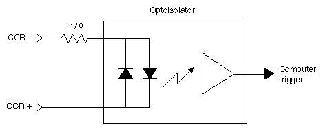
Table A-8 summarizes electrical specifications for the GPI receiver optoisolator.
Table A-8. GPI Receiver Input Optoisolator Electrical Specifications
Parameter | Value |
|---|---|
Forward voltage (VF) | 1.55 V, 1.2 V typical (IF = 10 mA) |
Continuous forward current (IF) | 30 mA |
Peak forward current | 1000 mA (10 us duration, 1% DC) |
Reverse current (IR) | 0.1 uA, 100 uA maximum (VR = 6 V) |
Isolation surge voltage (V10) | 2500 VACRMS (t = 1 min) |
The GPI receiver can be interfaced to the source equipment by tying either the CCR+ terminal or the CCR- terminal across the output terminals of an optoisolator, solid-state relay, or any device that acts like a single-pole contact switch. The other terminal (CCR- or CCR+) must then be appropriately tied to power or ground. Whenever the logic device is sourcing current (driving a logic high), a GPI trigger is generated.
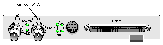
The GEN IN and GEN OUT BNC connectors on the HD I/O front panel provide a passive genlock loopthrough connection. If you attach a cable to one GEN connector, you must attach to the other GEN connector either a 75-ohm BNC terminator or a cable to other equipment accepting analog sync. If another cable is connected, it must be terminated at the end of the loopthrough chain. Figure A-7 shows the genlock BNCs.