This section includes:
Connectors' pinouts and baseboard locations
Information on baseboard jumpers
System I/O Addresses
System memory map addresses
Baseboard interrupts
Video modes
Figure 4-1 shows connector locations on the baseboard. This section provides pin information about the connectors.
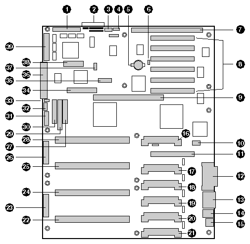
The baseboard (processor board) components are:
Wide SCSI B connector (J9J1)
System jumpers (J6J1)
Hard drive input LED connector (J6J3)
System speaker connector (J6J2)
Lithium battery (B4H1)
Wake on LAN technology connector (J4H1)
ISA slot (J1J1)
PCI slots B4 (closest to ISA), B3, B2, B1, A3, and A2 (farthest from ISA)
Memory module connector (J3G1)
ICMB connector (J1E1)
PCI slot A1 (J2D1)
Video and parallel port connectors (J1C1)
Serial port connector (J1B2)
Keyboard and mouse connectors (J1B1)
USB external connector (J1A1)
VRM connector for processor 4 (J4E1)
VRM connector for processors 4 and 3 (J4C2)
VRM connector for processor 3 (J4C1)
VRM connector for processor 2 (J4B1)
VRM connector for processors 2 and 1 (J4A2)
VRM connector for processor 1 (J4A1)
Processor 1 Slot 2 connector (J9A1)
Main power connector, primary (J9B1)
Processor 2 Slot 2 connector (J9B2)
Processor 3 Slot 2 connector (J9D1)
Main power connector, secondary (J9D2)
Front panel connector (J8E1)
Processor 4 Slot 2 connector (J9E1)
IDE connector (J9E2)
Diskette drive connector (J9E3)
Auxiliary power connector (J9E4)
USB internal header (JC9F14)
SMBus connector (J9F2)
F16 expansion connector (J7G1)
ITP connector (J6G1)
Narrow SCSI connector (J9H1)
External IPMB connector (J7H1)
SMM connector (J8H1)
Wide SCSI A connector (J9H2)
Figure 4-2 shows the pins on the main power connector. Table 4-1 lists the pin signal and color.
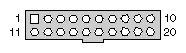
Table 4-1. Main Power Connector Pinouts
Pin | Signal | Wire Color |
|---|---|---|
1 | +3.3 VDC | Orange |
2 | +3.3 VDC | Orange |
3 | +3.3 VDC | Orange |
4 | COM | Black |
5 | COM | Black |
6 | COM | Black |
7 | COM | Black |
8 | +12 VDC | Yellow |
9 | +12 VDC | Yellow |
10 | +12 VDC | Yellow |
11 | +3.3 VDC | Orange |
12 | +3.3 VDC | Orange |
13 | +3.3 VDC | Orange |
14 | COM | Black |
15 | COM | Black |
16 | COM | Black |
17 | +5V Standby | Purple |
18 | +5 VDC | Red |
19 | +5 VDC | Red |
20 | +5 VDC | Red |
Figure 4-3 shows the auxiliary power connector. Table 4-2 lists the pin number and signal for each pin.
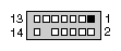
Table 4-2. Auxiliary Power Connector Pinouts
Pin | Signal |
|---|---|
1 | RTN_RS |
2 | 5V_RS |
3 | 3.3V_RS |
4 | FAN_SPEED |
5 | I2CSCL |
6 | I2CSDA |
7 | GND |
8 | SYS_PGOOD |
9 | PS_ON |
10 | GND |
11 | -12VCC |
12 | Key |
13 | 12V_RS |
14 | GND |
Figure 4-4 shows the diskette drive connector. Table 4-3 lists the diskette drive connector pinouts.
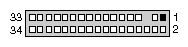
Table 4-3. Diskette Drive Connector Pinouts
Pin | Signal |
|---|---|
1 | GND |
2 | FD_DENSEL |
3 | GND |
4 | N/C |
5 | Key |
6 | FD_DRATE0 |
7 | GND |
8 | FD_INDEX_L |
9 | GND |
10 | FD_MTR0_L |
11 | GND |
12 | FD_DR1_L |
13 | GND |
14 | FD_DR0_L |
15 | GND |
16 | FD_MTR1_L |
17 | FD_MSEN1 |
18 | FD_DIR_L |
19 | GND |
20 | FD_STEP_L |
21 | GND |
22 | FD_WDATA_L |
23 | GND |
24 | FD_WGATE_L |
25 | GND |
26 | FD_TRK0_L |
27 | FD_MSEN0 |
28 | FD_WPROT_L |
29 | GND |
30 | FD_RDATA_L |
31 | GND |
32 | FD_HDSEL_L |
33 | GND |
34 | FD_DSKCHG_L |
A 30-pin connector attaches to the chassis front panel containing reset, NMI, sleep, and power control switches, LED indicators, and IPMB connection. Figure 4-5 shows the front panel connector. Table 4-4 lists the front panel connector pins and signals.
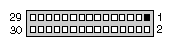
Table 4-4. Front Panel Connector Pinouts
Pin | Signal |
|---|---|
1 | SPEAKER_OUT |
2 | GND |
3 | CHASSIS_INTRUSI ON |
4 | FP_HD_ACT_L |
5 | +5V |
6 | SLEEP_CNTRL_l |
7 | FAN_FAILED_L |
8 | POWER_LED_L |
9 | POWER_FAULT_L |
10 | GND |
11 | I2C_SDA |
12 | NMI_FP_L |
13 | I2C_SCL |
14 | RST_FP_L |
15 | +5V standby |
16 | PWR_CNTRL_FP_L |
17 | FP_ISOL |
18 | GND |
19 | FAN_TACH(0) |
20 | FAN_TACH(1) |
21 | FAN_TACH(2) |
22 | FAN_TACH(3) |
23 | FAN_TACH(4) |
24 | FAN_TACH(5) |
25 | FAN_TACH(6) |
26 | FAN_TACH(7) |
27 | CLUSTER_LED |
28 | reserved |
29 | reserved |
30 | reserved |
Figure 4-6 shows the server management module (SMM) connector. Table 4-5 lists the SMM connector pinouts.
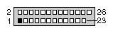
Table 4-5. Server Management Module Connector Pinouts
Pin | Signal | Description |
|---|---|---|
1 | CPU_SMI_L | System Management Interrupt |
2 | LOCAL_I2C_SCL | IPMB clock line |
3 | GND | Ground |
4 | Reserved | N/A |
5 | PWR_CNTRL_SFC_L | Host power supply on/off control |
6 | LOCAL_I2C_SDA | IPMB serial data line |
7 | 5VSTNDBY | +5V standby indication (power OK) |
8 | KEYLOCK_SFC_L | Keyboard lock signal |
9 | CPU_NMI | Nonmaskable interrupt indication |
10 | VCC3 | 3.3V power supply status input |
11 | RST_SFC_L | Baseboard reset signal from Server Monitor Module |
12 | GND | Ground |
13 | GND | Ground |
14 | Reserved | N/A |
15 | SECURE_MODE_BMC | Secure mode indication |
16 | GND | Ground |
17 | SFC_CHASSIS_INSTRUSION_L | Chassis intrusion indication |
18 | Reserved | N/A |
19 | Reserved | N/A |
20 | GND | Ground |
21 | Reserved | N/A |
22 | Reserved | N/A |
23 | Reserved | Not used |
24 | Reserved | N/A |
25 | Key pin (N/C) | Connector key |
26 | Reserved | N/A |

Figure 4-8 shows the system's VGA connector. Table 4-7 lists the pinouts for the VGA connector.
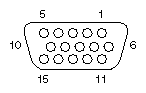
Table 4-7. Video Port Connector Pinouts
Pin | Signal |
|---|---|
1 | Red |
2 | Green |
3 | Blue |
4 | N/C |
5 | GND |
6 | GND |
7 | GND |
8 | GND |
10 | GND |
11 | NC |
12 | DDCDAT |
13 | HSYNC |
14 | VSYNC |
15 | DDCCLK |
Figure 4-9 shows the keyboard and mouse connector. Table 4-8 lists the connector pinouts for the keyboard and mouse connectors.
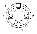
The PS/2-compatible connectors share a common housing, but they are functionally equivalent.
Table 4-8. Keyboard and Mouse Connector Pinouts
Pin | Keyboard signal | Mouse signal |
|---|---|---|
1 | KEYDAT | MSEDAT |
2 | NC | NC |
3 | GND | GND |
4 | FUSED_VCC (+5 V) | FUSED_VCC (+5 V) |
5 | KEYCLK | MSECLK |
6 | NC | NC |
Figure 4-10 shows the parallel port connection. Table 4-9 describes the parallel port connector pin signals.
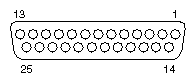
Table 4-9. Parallel Port Connector Pinout
Pin | Signal |
|---|---|
1 | STROBE_L |
2 | Data bit 0 |
3 | Data bit 1 |
4 | Data bit 2 |
5 | Data bit 3 |
6 | Data bit 4 |
7 | Data bit 5 |
8 | Data bit 6 |
9 | Data bit 7 |
10 | ACK_L |
11 | Busy |
12 | PE |
13 | SLCT |
14 | AUFDXT_L |
15 | ERROR_L |
16 | INIT_L |
17 | SLCTIN_L |
18-25 | GND |
Figure 4-11 shows the external serial port connector. Table 4-10 lists the serial port connector pin signals and functional descriptions.

Table 4-10. Serial Port A (External) Connector Pinout
Pin | Signal | Description |
|---|---|---|
1 | DCD | Data carrier detected |
2 | RXD | Receive data |
3 | TXD | Transmit data |
4 | DTR | Data terminal ready |
5 | GND | Ground |
6 | DSR | Data set ready |
7 | RTS | Request to send |
8 | CTS | Clear to send |
9 | RIA | Ring indication active |
The server provides a single, external Universal Serial Bus (USB) connector at the back panel (see Figure 4-12) and an internal header to be used with device bay expansion. Table 4-11 lists the pinouts for the external USB connector. Table 4-12 lists the pinouts for the internal USB header.

Table 4-11. USB External Connector Pinout
Pin | Signal | Notes |
|---|---|---|
1 | VCC | Cable power |
2 | Data - | Data (differential pair negative) |
3 | Data + | Data (differential pair positive) |
4 | GND | Cable ground |
Table 4-12. USB Internal Header Pinout
Pin | Signal | Notes |
|---|---|---|
1 |
| N/C |
2 | Data - | Data (differential pair negative) |
3 | Data + | Data (differential pair positive) |
4 | GND | Cable ground |
Figure 4-13 shows the server's narrow SCSI connector. Table 4-13 lists the narrow SCSI connection pinouts.
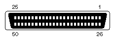
Table 4-13. Narrow SCSI Connector Pinouts
Pin | Signal |
|---|---|
1 | GND |
2 | SCD0_L |
3 | GND |
4 | SCD1_L |
5 | GND |
6 | SCD2_L |
7 | GND |
8 | SCD3_L |
9 | GND |
10 | SCD4_L |
11 | GND |
12 | SCD5_L |
13 | GND |
14 | SCD6_L |
15 | GND |
16 | SCD7_L |
17 | GND |
18 | SCDP_L |
19 | GND |
20 | GND |
21 | GND |
22 | GND |
23 | RESERVED |
24 | RESERVED |
25 | NC |
26 | TERMPWR |
27 | RESERVED |
28 | RESERVED |
29 | GND |
30 | GND |
31 | GND |
32 | SATN_L |
33 | GND |
34 | GND |
35 | GND |
36 | SBSY_L |
37 | GND |
38 | SACK_L |
39 | GND |
40 | SRESET_L |
41 | GND |
42 | SMSG_L |
43 | GND |
44 | SSEL_L |
45 | GND |
46 | SCD_L |
47 | GND |
48 | SREQ_L |
49 | GND |
50 | SIO_L |
Figure 4-14 shows the wide SCSI connector. Table 4-14 lists the wide SCSI pinouts and signal descriptions.
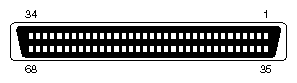
Table 4-14. Wide SCSI Connector Pinouts
Pin | Signal |
|---|---|
1-16 | GND |
17 | TERMPWR |
18 | TERMPWR |
19 | Reserved |
20-34 | GND |
35 | DB12_L |
36 | DB13_L |
37 | DB14_L |
38 | DB15_L |
39 | DBP1_L |
40 | DB0_L |
41 | DB1_L |
42 | DB2_L |
43 | DB3_L |
44 | DB4_L |
45 | DB5_L |
46 | DB6_L |
47 | DB7_L |
48 | DBP _L |
49-50 | GND |
51 | TERMPWR |
52 | TERMPWR |
53 | Reserved |
54 | GND |
55 | ATN_L |
56 | GND |
57 | BSY_L |
58 | ACK_L |
59 | RST_L |
60 | MSG_L |
61 | SEL_L |
62 | C/D_L |
63 | REQ_L |
64 | I/O_L |
65 | DB8_L |
66 | DB9_L |
67 | DB10_L |
68 | DB11_L |
Figure 4-15 shows the server's internal IDE connector. Table 4-15 lists the connectors and signals for the internal IDE connector. If no IDE drives are present, no IDE cable should be connected. If only one IDE drive is installed, it must be connected at the end of the cable.
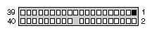
Table 4-15. IDE Connector Pinouts
Pin | Signal |
|---|---|
1 | RESET_L |
2 | GND |
3 | DD7 |
4 | DD8 |
5 | DD6 |
6 | DD9 |
7 | DD5 |
8 | DD10 |
9 | DD4 |
10 | DD11 |
11 | DD3 |
12 | DD12 |
13 | DD2 |
14 | DD13 |
15 | DD1 |
16 | DD14 |
17 | DD0 |
18 | DD15 |
19 | GND |
20 | Keyed |
21 | IDEDRQ |
22 | GND |
23 | DIOW_L |
24 | GND |
25 | DIOR_L |
26 | GND |
27 | IORDY |
28 | CSEL (1 KΩ p/d) |
29 | IDEDAK_L |
30 | GND |
31 | IDEIRQ |
32 | Reserved (N/C) |
33 | IDESA1 |
34 | PDIAG_L (tied to GND) |
35 | IDESA0 |
36 | IDESA2 |
37 | IDECS1_L |
38 | IDECS3_L |
39 | IDEHDACT_L |
40 | GND |
Figure 4-16 shows the hard drive LED connector. Table 4-16 lists the pins and signals for the hard drive LED connector.

Table 4-17 lists the ISA connector pinouts and signal names.
Table 4-17. ISA Connector Pinouts
Pin | Signal |
|---|---|
A1 | IOCHK_L |
A2 | SD7 |
A3 | SD6 |
A4 | SD5 |
A5 | SD4 |
A6 | SD3 |
A7 | SD2 |
A8 | SD1 |
A9 | SD0 |
A10 | IOCHRDY |
A11 | AEN |
A12 | SA19 |
A13 | SA18 |
A14 | SA17 |
A15 | SA16 |
A16 | SA15 |
A17 | SA14 |
A18 | SA13 |
A19 | SA12 |
A20 | SA11 |
A21 | SA10 |
A22 | SA9 |
A23 | SA8 |
A24 | SA7 |
A25 | SA6 |
A26 | SA5 |
A27 | SA4 |
A28 | SA3 |
A29 | SA2 |
A30 | SA1 |
A31 | SA0 |
B1 | GND |
B2 | RESET |
B3 | +5V |
B4 | IRQ9 |
B5 | -5V |
B6 | DRQ2 |
B7 | -12V |
B8 | SRDY_L |
B9 | +12V |
B10 | GND |
B11 | SMEMW_L |
B12 | SMEMR_L |
B13 | IOW_L |
B14 | IOR_L |
B15 | DACK3_L |
B16 | DRQ3 |
B17 | DACK1_L |
B18 | DRQ1 |
B19 | REFRESH_L |
B20 | BCLK |
B21 | IRQ7 |
B22 | IRQ6 |
B23 | IRQ5 |
B24 | IRQ4 |
B25 | IRQ3 |
B26 | DACK2_L |
B27 | TC |
B28 | BALE |
B29 | +5V |
B30 | OSC |
B31 | GND |
Connector key |
|
C1 | SBHE_L |
C2 | LA23 |
C3 | LA22 |
C4 | LA21 |
C5 | LA20 |
C6 | LA19 |
C7 | LA18 |
C8 | LA17 |
C9 | MEMR_L |
C10 | MEMW_L |
C11 | SD8 |
C12 | SD9 |
C13 | SD10 |
C14 | SD11 |
C15 | SD12 |
C16 | SD13 |
C17 | SD14 |
C18 | SD15 |
Connector key |
|
D1 | MEMCS16_L |
D2 | IOCS16_L |
D3 | IRQ10 |
D4 | IRQ11 |
D5 | IRQ12 |
D6 | IRQ15 |
D7 | IRQ14 |
D8 | DACK0_L |
D9 | DRQ0 |
D10 | DACK5_L |
D11 | DRQ5 |
D12 | DACK6_L |
D13 | DRQ6 |
D14 | DACK7_L |
D15 | DRQ7 |
D16 | +5V |
D17 | MASTER16_L |
D18 | GND |
Table 4-18 provides the PCI connector pinouts and lists the signal value.
 | Note: The baseboard does not provide a PCI 3.3 V power connector. Only the 5 V PCI signaling environment is supported, and no power is available at the 3.3 V signal pins in expansion slots. |
Table 4-18. PCI Connector Pinouts
Pin | Signal |
|---|---|
A1 | TRST_L |
A2 | +12 V |
A3 | TMS |
A4 | TDI |
A5 | +5 V |
A6 | INTA_L |
A7 | INTC_L |
A8 | +5 V |
A9 | Reserved |
A10 | +5 V |
A11 | Reserved |
A12 | GND |
A13 | GND |
A14 | Reserved |
A15 | RST_L |
A16 | +5 V |
A17 | GNT_L |
A18 | GND |
A19 | Reserved |
A20 | AD30 |
A21 | +3.3 V * |
A22 | AD28 |
A23 | AD26 |
A24 | GND |
A25 | AD24 |
A26 | IDSEL |
A27 | +3.3 V * |
A28 | AD22 |
A29 | AD20 |
A30 | GND |
A31 | AD18 |
A32 | AD16 |
A33 | +3.3 V * |
A34 | FRAME_L |
A35 | GND |
A36 | TRDY_L |
A37 | GND |
A38 | STOP_L |
A39 | +3.3 V * |
A40 | SDONE |
A41 | SBO_L |
A42 | GND |
A43 | PAR |
A44 | AD15 |
A45 | +3.3 V * |
A46 | AD13 |
A47 | AD11 |
A48 | GND |
A49 | AD9 |
A50 | KEY |
A51 | KEY |
A52 | C/BE0_L |
A53 | +3.3 V * |
A54 | AD6 |
A55 | AD4 |
A56 | GND |
A57 | AD2 |
A58 | AD0 |
A59 | +5 V |
A60 | REQ64_L |
A61 | +5 V |
A62 | +5 V |
B1 | -12 V |
B2 | TCK |
B3 | GND |
B4 | TD0 (NC) |
B5 | +5 V |
B6 | +5 V |
B7 | INTB_L |
B8 | INTD_L |
B9 | PRSNT1_L |
B10 | Reserved |
B11 | PRSNT2_L |
B12 | GND |
B13 | GND |
B14 | Reserved |
B15 | GND |
B16 | PCICLK |
B17 | GND |
B18 | REQ_L |
B19 | +5 V |
B20 | AD31 |
B21 | AD29 |
B22 | GND |
B23 | AD27 |
B24 | AD25 |
B25 | +3.3 V * |
B26 | C/BE3_L |
B27 | AD23 |
B28 | GND |
B29 | AD21 |
B30 | AD19 |
B31 | +3.3 V * |
B32 | AD17 |
B33 | C/BE2_L |
B34 | GND |
B35 | IRDY_L |
B36 | +3.3 V * |
B37 | DEVSEL_L |
B38 | GND |
B39 | LOCK_L |
B40 | PERR_L |
B41 | +3.3 V * |
B42 | SERR_L |
B43 | +3.3 V * |
B44 | C/BE1_L |
B45 | AD14 |
B46 | GND |
B47 | AD12 |
B48 | AD10 |
B49 | GND |
B50 | KEY |
B51 | KEY |
B52 | AD8 |
B53 | AD7 |
B54 | +3.3 V * |
B55 | AD5 |
B56 | AD3 |
B57 | GND |
B58 | AD1 |
B59 | +5 V |
B60 | ACK64_L |
B61 | +5 V |
B62 | +5 V |
One 11-pin single inline header provides three 3-pin jumper blocks that control various configuration options. Figure 4-17 shows the location. Items shown in bold in Table 4-19 show default placement for each configurable option.
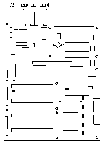
Table 4-19. Baseboard Jumper Summary
Function | Pins (default in bold) | What it does at system reset |
|---|---|---|
1-2, BMC Control | Preserves the contents of NVRAM. | |
| 2-3, Force Erase | Replaces the contents of NVRAM with the manufacturing default settings. |
5-6, Protect | Maintains the current system password. | |
| 6-7, Erase | Clears the password. |
9-10, Normal | System attempts to boot using the BIOS stored in flash memory. | |
| 10-11, Recovery | BIOS attempts a recovery boot, loading BIOS code from a diskette into the flash device. This is typically used when the BIOS code has been corrupted. |
The short general procedure for changing a configuration setting is the same for most of the jumper functions, and is described in the following steps.
Read and observe the safety and ESD precautions at the beginning of Chapter 1.
Turn off all connected peripherals, turn off system power, and disconnect all AC power cords.
Remove the access cover. You do not need to remove the baseboard from the chassis, and you probably do not need to remove any add-in boards.
Locate the configuration jumpers at the edge of the baseboard toward the front of the system, near the narrow SCSI connector.
Move jumper to pins specified for the desired setting.
Reinstall the access cover using the original screws, connect the power cords, and turn on the system for the change to take effect.
You may need to repeat these steps to move the jumper back to its original setting, depending on the jumper function.
The jumper at pins 1, 2, and 3 controls whether settings stored in CMOS nonvolatile memory (NVRAM) are retained during a system reset.
Procedure to restore the system's CMOS and RTC to default values:
Move the CMOS jumper from pins 1 and 2 to pins 2 and 3 (the Clear CMOS memory position).
Reinstall the access cover for your safety (using the original screws), and connect the power cords to the system.
Turn the system on. Wait for POST to complete and for the messages “NVRAM cleared by jumper” and “Press F2 to enter Setup” to appear. This automatically reprograms CMOS and RTC to their default settings, except for the password.
Enter Setup and make any changes necessary (for example, changing the boot device). Press F10 to save the new Setup configuration and exit Setup.
Turn off the system, and disconnect all AC power cords from the system.
Again remove the access cover.
Move the jumper from pins 2 and 3 back to pins 1 and 2 (the Protect CMOS memory position).
Reinstall the access cover using the original screws, and connect the power cords to the system.
Run BIOS Setup or the SSU to verify the correct settings. See Chapter 3 in the SGI 1400 Server Family User's Guide.
The jumper at pins 5, 6, and 7 controls whether a stored password is retained or cleared during a system reset.
Procedure to clear the current password and then enter a new one:
Move the Password jumper from pins 5 and 6 to pins 6 and 7.
Reinstall the access cover for your safety (using the original screws), and connect the power cords to the system.
Turn the system on, and wait for POST to complete. This automatically clears the password.
Turn off the system, and disconnect all AC power cords.
Again remove the access cover.
Move the jumper from pins 6 and 7 back to pins 5 and 6.
Reinstall the access cover using the original screws, and connect the power cords to the system.
Run the SSU to specify a new password. See Chapter 3 in the SGI 1400 Server Family User's Guide.
The jumper at pins 9, 10, and 11 controls whether the system attempts to boot using the BIOS programmed in flash memory.
The following steps disable recovery booting:
Move the recovery boot jumper from pins 9 and 10 to pins 10 and 11.
Reinstall the access cover for your safety (using the original screws), then connect the power cords to the system.
Turn the system on, and insert the Flash Memory Update Utility diskette in drive A. After the system boots, the speaker emits a single beep and the recovery process starts. This takes about three minutes. When the recovery process completes, the speaker emits two beeps.
While in the recovery mode, there is no screen display on the monitor. The keyboard is disabled as the system automatically recovers the BIOS. The beep codes listed in Table 4-20 describe the recovery status.
Table 4-20. BIOS Recovery Beep Codes
Beep Code | Message |
|---|---|
2 | Successful completion, no errors. |
4 | The system could not boot from the diskette. The diskette may not be bootable. |
Continuous series of low beeps | The wrong BIOS recovery files are being used and/or the flash memory jumper is in the wrong position. |
Turn the system off, disconnect all AC power cords from the system, and remove the access cover.
Move the jumper from pins 10 and 11 back to pins 9 and 10 to enable the normal boot mode.
Replace the access cover, remove the diskette from drive A, and connect the power cords to the system.
After running the special recovery mode, run the SSU to specify a new password. See Chapter 3 in the SGI 1400 Server Family User's Guide.
Table 4-21 shows the location in I/O space of all directly I/O–accessible registers.
Table 4-21. System I/O Addresses
Address(es) | Resource | Device | Notes |
|---|---|---|---|
0000h - 000Fh | DMA Controller 1 | PIIX4E |
|
0010h - 001Fh | DMA Controller 1 | PIIX4E | Aliased from 0000h - 000Fh |
0020h - 0021h | Interrupt Controller 1 | PIIX4E |
|
0022h - 0023h |
|
|
|
0024h - 0025h | Interrupt Controller 1 | PIIX4E | Aliased from 0020h - 0021h |
0026h - 0027h |
|
|
|
0028h - 0029h | Interrupt Controller 1 | PIIX4E | Aliased from 0020h - 0021h |
002Ah - 002Bh |
|
|
|
002Ch - 002Dh | Interrupt Controller 1 | PIIX4E | Aliased from 0020h - 0021h |
002Eh - 002Fh | Super I/O Index and Data Ports |
|
|
0030h - 0031h | Interrupt Controller 1 | PIIX4E | Aliased from 0020h - 0021h |
0032h - 0033h |
|
|
|
0034h - 0035h | Interrupt Controller 1 | PIIX4E | Aliased from 0020h - 0021h |
0036h - 0037h |
|
|
|
0038h - 0039h | Interrupt Controller 1 | PIIX4E | Aliased from 0020h - 0021h |
003Ah - 003Bh |
|
|
|
003Ch - 003Dh | Interrupt Controller 1 | PIIX4E | Aliased from 0020h - 0021h |
003Eh - 003Fh |
|
|
|
0040h - 0043h | Programmable Timers | PIIX4E |
|
0044h - 004Fh |
|
|
|
0050h - 0053h | Programmable Timers | PIIX4E | Aliased from 0040h - 0043h |
0054h - 005Fh |
|
|
|
0060h, 0064h | Keyboard Controller |
| Keyboard chip select from 87307 |
0061h | NMI Status & Control Register | PIIX4E |
|
0063h | NMI Status & Control Register | PIIX4E | Aliased |
0065h | NMI Status & Control Register | PIIX4E | Aliased |
0067h | NMI Status & Control Register | PIIX4E | Aliased |
0070h | NMI Mask (bit 7) & RTC Address (bits 6::0) | PIIX4E |
|
0072h | NMI Mask (bit 7) & RTC Address (bits 6::0) | PIIX4E | Aliased from 0070h |
0074h | NMI Mask (bit 7) & RTC Address (bits 6::0) | PIIX4E | Aliased from 0070h |
0076h | NMI Mask (bit 7) & RTC Address (bits 6::0) | PIIX4E | Aliased from 0070h |
0071h | RTC Data | PIIX4E |
|
0073h | RTC Data | PIIX4E | Aliased from 0071h |
0075h | RTC Data | PIIX4E | Aliased from 0071h |
0077h | RTC Data | PIIX4E | Aliased from 0071h |
0080h - 008Fh | DMA Low Page Register | PIIX4E |
|
0090h - 0091h | DMA Low Page Register (aliased) | PIIX4E |
|
0092h | System Control Port A (PC–AT control Port) (this port not aliased in DMA range) | PIIX4E |
|
0093h - 009Fh | DMA Low Page Register (aliased) | PIIX4E |
|
0094h | Video Display Controller |
|
|
00A0h - 00A1h | Interrupt Controller 2 | PIIX4E |
|
00A4h - 00A15 | Interrupt Controller 2 (aliased) | PIIX4E |
|
00A8h - 00A19 | Interrupt Controller 2 (aliased) | PIIX4E |
|
00Ach - 00Adh | Interrupt Controller 2 (aliased) | PIIX4E |
|
00B0h - 00B1h | Interrupt Controller 2 (aliased) | PIIX4E |
|
00B2h | Advanced Power Management Control | PIIX4E |
|
00B3h | Advanced Power Management Status | PIIX4E |
|
00B4h - 00B5h | Interrupt Controller 2 (aliased) | PIIX4E |
|
00B8h - 00B9h | Interrupt Controller 2 (aliased) | PIIX4E |
|
00BCh - 00BDh | Interrupt Controller 2 (aliased) | PIIX4E |
|
00C0h - 00DFh | DMA Controller 2 | PIIX4E |
|
00F0h | Clear NPX error |
| Resets IRQ13 |
00F8h - 00FFh | x87 Numeric Coprocessor |
|
|
0102h | Video Display Controller |
|
|
0170h - 0177h | Secondary Fixed Disk Controller (IDE) | PIIX4E | Not used |
01F0h - 01F7h | Primary Fixed Disk Controller (IDE) | PIIX4E |
|
0200h - 0207h | Game I/O Port |
| Not used |
0220h - 022Fh | Serial Port A |
|
|
0238h - 023Fh | Serial Port B |
|
|
0278h - 027Fh | Parallel Port 3 |
|
|
02E8h - 02Efh | Serial Port B |
|
|
02F8h - 02FFh | Serial Port B |
|
|
0338h - 033Fh | Serial Port B |
|
|
0370h - 0375h | Secondary Diskette |
|
|
0376h | Secondary IDE |
|
|
0377h | Secondary IDE/Diskette |
|
|
0378h - 037Fh | Parallel Port 2 |
|
|
03B4h - 03Bah | Monochrome Display Port |
|
|
03BCh - 03BFh | Parallel Port 1 (Primary) |
|
|
03C0h - 03CFh | Video Display Controller |
|
|
03D4h - 03DAh | Color Graphics Controller |
|
|
03E8h - 03EFh | Serial Port A |
|
|
03F0h - 03F5h | Diskette Controller |
|
|
03F6h - 03F7h | Primary IDE - Sec. Diskette |
|
|
03F8h - 03FFh | Serial Port A (Primary) |
|
|
0400h - 043Fh | DMA Controller 1, Extended Mode Registers | PIIX4E |
|
04D0h - 04D1h | Interrupt Controllers 1 and 2 Control Register |
|
|
0678h - 067Ah | Parallel Port (ECP) |
|
|
0778h - 077Ah | Parallel Port (ECP) |
|
|
07BCh - 07BEh | Parallel Port (ECP) |
|
|
0CA0 - CA3h | BMC Registers |
|
|
0CF8h | PCI CONFIG_ADDRESS Register |
| Located in 450NX |
0CF9h | NBX Turbo and Reset control | PIIX4E |
|
0CFCh | PCI CONFIG_DATA Register |
| Located in 450NX |
46E8h | Video Display Controller |
|
|
Table 4-22 lists the memory map address ranges and the functions they support.
Table 4-22. Memory Map Address Range
Address Range (hex) | Amount | Function |
|---|---|---|
0 to 07FFFFh | 640 KB | DOS region, base system memory |
0A0000h to 0BFFFFh | 128 KB | Video or SMM memory |
0C0000h and 0DFFFFh | 128 KB | Add-in board BIOS and buffer area |
0E0000h to 0FFFFFh | 128 KB | System BIOS |
0E0000h to 0EFFFFh | 2 MB | Extended system BIOS |
FC000000h to FFFFFFFFh | 64 MB | PCI memory space |
Table 4-23 recommends the logical interrupt mapping of interrupt sources; it reflects a typical configuration, but these interrupts can be changed by the user. Use the information to determine how to program each interrupt. The actual interrupt map is defined using configuration registers in the PIIX4E and the I/O controller. I/O Redirection Registers in the I/O APIC are provided for each interrupt signal; the signals define hardware interrupt signal characteristics for APIC messages sent to local APIC(s).
| Note: To disable either IDE controller and reuse the interrupt: if you plan to disable either IDE controller to reuse the interrupt for that controller, you must physically unplug the IDE cable from the board connector (IDE0) if a cable is present. Simply disabling the drive by configuring the SSU option does not make the interrupt available. |
Table 4-23. Interrupt I/O Descriptions
Interrupt | I/O APIC level | Description |
|---|---|---|
INTR | INT0 | Processor interrupt |
NMI | N/A | NMI from PIC to processor |
IRQ1 | INT1 | Keyboard interrupt |
Cascade | INT2 | Interrupt signal from second 8259 in PIIX4E |
IRQ3 | INT3 | Serial port A or B interrupt from SIO device (user can configure) |
IRQ4 | INT4 | Serial port A or B interrupt from SIO device (user can configure) |
IRQ5 | INT5 | Parallel port II |
IRQ6 | INT6 | Diskette port |
IRQ7 | INT7 | Parallel port |
IRQ8_L | INT8 | RTC interrupt |
IRQ9 | INT9 | Signal control interrupt (SCI) used by ACPI-compliant OS |
IRQ10 | INT10 |
|
IRQ11 | INT11 |
|
IRQ12 | INT12 | Mouse interrupt |
| INT13 |
|
IRQ14 | INT14 | Compatibility IDE interrupt from primary channel IDE devices 0 and 1 |
IRQ15 | INT15 |
|
SMI_L |
| System management interrupt—general purpose indicator sourced by the PIIX4E and BMC through the PID to the processors |
The CL-GD5480 integrated video controller provides all standard IBM VGA modes. With 2 MB of SGRAM standard, the system supports special Cirrus Logic extended modes. Table 4-24 and Table 4-25 list the standard and extended modes that this implementation supports, including the number of colors and palette size (e.g., 16 colors out of 256 K colors), resolution, pixel frequency, and scan frequencies.
Table 4-24. Standard VGA Modes
Mode(s) in Hex | Bits per pixel | Colors (no per palette size) | Resolution | Pixel Freq. (MHz) | Horizontal Freq. (kHz) | Vertical Freq. (Hz) |
|---|---|---|---|---|---|---|
0, 1 | 4 | 16/256K | 360 X 400 | 14 | 31.5 | 70 |
2, 3 | 4 | 16/256K | 720 X 400 | 28 | 31.5 | 70 |
4, 5 | 4 | 4/256K | 320 X 200 | 12.5 | 31.5 | 70 |
6 | 4 | 2/256K | 640 X 200 | 25 | 31.5 | 70 |
7 | 4 | Mono | 720 X 400 | 28 | 31.5 | 70 |
D | 4 | 16/256K | 320 X 200 | 12.5 | 31.5 | 70 |
E | 4 | 16/256K | 640 X 200 | 25 | 31.5 | 70 |
F | 4 | Mono | 640 X 350 | 25 | 31.5 | 70 |
10 | 4 | 16/256K | 640 X 350 | 25 | 31.5 | 70 |
11 | 4 | 2/256K | 640 X 480 | 25 | 31.5 | 60 |
12 | 4 | 16/256K | 640 X 480 | 25 | 31.5 | 60 |
12+ | 4 | 16/256K | 640 X 480 | 31.5 | 37.5 | 75 |
13 | 8 | 256/256K | 320 X 200 | 12.5 | 31.5 | 70 |
Table 4-25. Extended VGA Modes
Mode(s) in Hex | Bits per pixel | Colors | Resolution | Pixel Freq. (MHz) | Horiz. Freq. (KHz) | Vert. Freq. (Hz) | Memory |
|---|---|---|---|---|---|---|---|
58, 6A | 8 | 16/256K | 800 X 600 | 36 | 35.2 | 56 | 1MB |
58, 6A | 8 | 16/256K | 800 X 600 | 40 | 37.8 | 60 | 1MB |
58, 6A | 8 | 16/256K | 800 X 600 | 50 | 48.1 | 72 | 1MB |
58, 6A | 8 | 16/256K | 800 X 600 | 49.5 | 46.9 | 75 | 1MB |
5C | 8 | 256/256K | 800 X 600 | 36 | 35.2 | 56 | 1MB |
5C | 8 | 256/256K | 800 X 600 | 40 | 37.9 | 60 | 1MB |
5C | 8 | 256/256K | 800 X 600 | 50 | 48.1 | 72 | 1MB |
5C | 8 | 256/256K | 800 X 600 | 49.5 | 46.9 | 75 | 1MB |
5C | 8 | 256/256K | 800 X 600 | 56.25 | 53.7 | 85 | 1MB |
5C | 8 | 256/256K | 800 X 600 | 68.2 | 63.6 | 100 | 1MB |
5D | 8 | 16/256K (interlaced) | 1024 X 768 | 44.9 | 35.5 | 43 | 1MB |
5D | 8 | 16/256K | 1024 X 768 | 65 | 48.3 | 60 | 1MB |
5D | 8 | 16/256K | 1024 X 768 | 75 | 56 | 70 | 1MB |
5D | 8 | 16/256K | 1024 X 768 | 78.7 | 60 | 75 | 1MB |
5E | 8 | 256/256K | 640 X 400 | 25 | 31.5 | 70 | 1MB |
5F | 8 | 256/256K | 640 X 480 | 25 | 31.5 | 60 | 1MB |
5F | 8 | 256/256K | 640 X 480 | 31.5 | 37.9 | 72 | 1MB |
5F | 8 | 256/256K | 640 X 480 | 31.5 | 37.5 | 75 | 1MB |
5F | 8 | 256/256K | 640 X 480 | 36 | 43.3 | 85 | 1MB |
5F | 8 | 256/256K | 640 X 480 | 43.2 | 50.9 | 100 | 1MB |
60 | 8 | 256/256K (interlaced) | 1024 X 768 | 44.9 | 35.5 | 43 | 1MB |
60 | 8 | 256/256K | 1024 X 768 | 65 | 48.3 | 60 | 1MB |
60 | 8 | 256/256K | 1024 X 768 | 75 | 56 | 70 | 1MB |
60 | 8 | 256/256K | 1024 X 768 | 78.7 | 60 | 75 | 1MB |
60 | 8 | 256/256K | 1024 X 768 | 94.5 | 68.3 | 85 | 1MB |
60 | 8 | 256/256K | 1024 X 768 | 113.3 | 81.4 | 100 | 1MB |
64 | 16 | 64K | 640 X 480 | 25 | 31.5 | 60 | 1MB |
64 | 16 | 64K | 640 X 480 | 31.5 | 37.9 | 72 | 1MB |
64 | 16 | 64K | 640 X 480 | 31.5 | 37.5 | 75 | 1MB |
64 | 16 | 64K | 640 X 480 | 36 | 43.3 | 85 | 1MB |
64 | 16 | 64K | 640 X 480 | 43.2 | 50.9 | 100 | 1MB |
65 | 16 | 64K | 800 X 600 | 36 | 35.2 | 56 | 1MB |
65 | 16 | 64K | 800 X 600 | 40 | 37.8 | 60 | 1MB |
65 | 16 | 64K | 800 X 600 | 50 | 48.1 | 72 | 1MB |
65 | 16 | 64K | 800 X 600 | 49.5 | 46.9 | 75 | 1MB |
65 | 16 | 64K | 800 X 600 | 56.25 | 53.7 | 85 | 1MB |
65 | 16 | 64K | 800 X 600 | 68.2 | 63.6 | 100 | 1MB |
66 | 16 | 32K | 640 X 480 | 25 | 31.5 | 60 | 1MB |
66 | 16 | 32K | 640 X 480 | 31.5 | 37.9 | 72 | 1MB |
66 | 16 | 32K | 640 X 480 | 31.5 | 37.5 | 75 | 1MB |
66 | 16 | 32K | 640 X 480 | 36 | 43.3 | 85 | 1MB |
66 | 16 | 32K | 640 X 480 | 43.2 | 50.9 | 100 | 1MB |
67 | 16 | 32K | 800 X 600 | 36 | 35.2 | 56 | 1MB |
67 | 16 | 32K | 800 X 600 | 40 | 37.8 | 60 | 1MB |
67 | 16 | 32K | 800 X 600 | 50 | 48.1 | 72 | 1MB |
67 | 16 | 32K | 800 X 600 | 49.5 | 46.9 | 75 | 1MB |
67 | 16 | 32K | 800 X 600 | 56.25 | 53.7 | 85 | 1MB |
67 | 16 | 32K | 800 X 600 | 68.2 | 63.6 | 100 | 1MB |
68 | 16 | 32K (interlaced) | 1024 X 768 | 44.9 | 35.5 | 43 | 2MB |
68 | 16 | 32K | 1024 X 768 | 65 | 48.3 | 60 | 2MB |
68 | 16 | 32K | 1024 X 768 | 75 | 56 | 70 | 2MB |
68 | 16 | 32K | 1024 X 768 | 78.7 | 60 | 75 | 2MB |
68 | 16 | 32K | 1024 X 768 | 94.5 | 68.3 | 85 | 2MB |
68 | 16 | 32K | 1024 X 768 | 113.3 | 81.4 | 100 | 2MB |
6C | 8 | 16/256K (interlaced) | 1280 X 1024 | 75 | 48 | 43 | 1MB |
6D | 8 | 256/256K (interlaced) | 1280 X 1024 | 75 | 48 | 43 | 2MB |
6D | 8 | 256/256K | 1280 X 1024 | 108 | 65 | 60 | 2MB |
6D | 8 | 256/256K | 1280 X 1024 | 135 | 80 | 75 | 2MB |
6D | 8 | 256/256K | 1280 X 1024 | 157.5 | 91 | 85 | 2MB |
6E | 16 | 32K | 1152 X 864 | 94.5 | 63.9 | 70 | 2MB |
6E | 16 | 32K | 1152 X 864 | 108 | 67.5 | 75 | 2MB |
6E | 16 | 32K | 1152 X 864 | 121.5 | 76.7 | 85 | 2MB |
6E | 16 | 32K | 1152 X 864 | 143.5 | 91.5 | 100 | 2MB |
71 | 24 | 16M | 640 X 480 | 25 | 31.5 | 60 | 1MB |
71 | 24 | 16M | 640 X 480 | 31.5 | 37.9 | 72 | 1MB |
71 | 24 | 16M | 640 X 480 | 31.5 | 37.5 | 75 | 1MB |
71 | 24 | 16M | 640 X 480 | 36 | 43.3 | 85 | 1MB |
71 | 24 | 16M | 640 X 480 | 43.2 | 50.9 | 100 | 1MB |
74 | 16 | 64K (interlaced) | 1024 X 768 | 44.9 | 35.5 | 43 | 2MB |
74 | 16 | 64K | 1024 X 768 | 65 | 48.3 | 60 | 2MB |
74 | 16 | 64K | 1024 X 768 | 75 | 56 | 70 | 2MB |
74 | 16 | 64K | 1024 X 768 | 78.7 | 60 | 75 | 2MB |
74 | 16 | 64K | 1024 X 768 | 94.5 | 68.3 | 85 | 2MB |
74 | 16 | 64K | 1024 X 768 | 113.3 | 81.4 | 100 | 2MB |
78 | 16 | 32K | 800 X 600 | 36 | 35.2 | 56 | 1MB |
78 | 24 | 16M | 800 X 600 | 40 | 37.8 | 60 | 2MB |
78 | 24 | 16M | 800 X 600 | 50 | 48.1 | 72 | 2MB |
78 | 24 | 16M | 800 X 600 | 49.5 | 46.9 | 75 | 2MB |
78 | 24 | 16M | 800 X 600 | 56.25 | 53.7 | 85 | 2MB |
78 | 24 | 16M | 800 X 600 | 68.2 | 63.6 | 100 | 2MB |
7B | 8 | 256/256K (interlaced) | 1600 X 1200 | 135 | 62.5 | 48 | 2MB |
7B | 8 | 256/256K | 1600 X 1200 | 162 | 75 | 60 | 2MB |
7C | 8 | 256/256K | 1152 X 864 | 94.5 | 63.9 | 70 | 1MB |
7C | 8 | 256/256K | 1152 X 864 | 108 | 67.5 | 75 | 1MB |
7C | 8 | 256/256K | 1152 X 864 | 121.5 | 76.7 | 85 | 1MB |
7C | 8 | 256/256K | 1152 X 864 | 143.5 | 91.5 | 100 | 1MB |
7D | 16 | 64K | 1152 X 864 | 94.5 | 63.9 | 70 | 2MB |
7D | 16 | 64K | 1152 X 864 | 108 | 67.5 | 75 | 2MB |
7D | 16 | 64K | 1152 X 864 | 121.5 | 76.7 | 85 | 2MB |
7D | 16 | 64K | 1152 X 864 | 143.5 | 91.5 | 100 | 2MB |