The FDDIXPress network controller board is a RISC-based, high-performance node processor that connects the host to an FDDI network and processes the transmission and reception of data across the network.
Features of the controller board include:
AMD SUPERNET Chip Set
The FDDIXPress Controller board uses a subset of this chip set.1 MB Communications Buffer
The Controller board has a one-megabyte communications buffer to help eliminate data overrun.On-Board RISC Processor
AMD's Am29000 RISC microprocessor is capable of operating at 14 MIPS (millions of instructions/second).High-Performance VMEbus Interface
The contoller board uses high-speed FIFO memory buffers and an asynchronous state machine that monitors VMEbus signalling.
Refer to Figure 4-1 during the following discussion.
The optical interface is provided by the Am7984A ENDEC and the Am7985A EDS . The optic interface chips connect directly to the optic transmitter and receiver through differential ECL drivers and receivers in the ENDEC and EDS parts.
An I/O port with high current sink capability is provided for controlling an external optical bypass switch. The switch bypasses the board in the case of a power failure. It can also take the node off the ring for diagnostic purposes, without causing the ring to wrap.
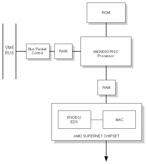
The ENDEC component implements the 4B/5B encoding/decoding as specified by the ANSI X3T9.5 FDDI standard. It supports a 100 Mbps data rate with a 125 Mbaud serial output, and incorporates an internal elastic store buffer to compensate for clock mismatch. It also regenerates the incoming data string for transmission to the next host on the ring and inserts idle symbols into the stream if error is detected. The Am7984/Am7985A supports selectable loopback and repeat modes.
The EDS contains the clock generator, the Phase Lock Loop, and the data retimer. The clock inputs are selectable from a crystal, a TTL clock source, or a differential BCLK (byte clock). The data retimer removes the jitter component from the recovered data and aligns it with the negative of the recovered clock. The encoded output is selectable as NRZ or NRZI.
An I/O port with high current sink capability (up to 400 ma) is provided for controlling an external optical bypass switch. The port is available to the user via a right 2X2 Berg connector near the VMEbus front panel.
The AMD media access control (MAC) chip is the Am79C83 FORMAC. The main function of the MAC controller is to provide access to the FDDI network. The MAC is responsible for receiving incoming frames as well as capturing the token for transmitting frames.
In the receive mode, the MAC does the following:
strips away the physical layer headers before sending the frame to the receive FIFO
compares the destination address, and notifies the Rx State machine if the destination address does not match
performs a CRC on the frame
generates status bits that identify receiver line conditions and frame status, and strips away the end-of-frame characters
compares the source address field
If the FORMAC identifies the source address as its own, it strips the remaining characters from the ring and replaces them with an idle pattern. Provision is made for using content addressable memory for decoding group addresses. The FORMAC supplies two 8-bit data buses parity (rx and tx) for buffer memory storage; the rx bus is tri-stateable.
In the transmit mode, the FORMAC captures the token, generates the physical layer headers, supplies the source address, generates the frame check sequence (CRC), and provides the ending delimiter and frame status.
The FORMAC also supplies the control for performing external source and destination address detection circuitry. This is necessary in bridging applications where the destination address is not present on the original FDDI ring. Signals are also present for generating ring statistics (such as error counts, line conditions, and so on).
The FORMAC contains the timers required to regulate the operation of the ring. These timers determine the length of time the host can hold the token (THT), the average time it takes the token to circulate around the ring (TRT), and a valid-transmission timer (TVX) to recover from transient ring error situations.
The buffer memory is an interim storage area for received frames and is used to buffer packets for transmission. It is composed of four sections: the DMA controller gate array, the elastic store buffer, the dynamic RAM controller and page-mode state machine, and the video DRAM memory.
The buffer memory consists of 1 MB of video dynamic RAM. Access to the random side of the memory is available by the Am29K microprocessor, the DMA controller gate array, and the VMEbus. Access to the serial side is available to the BUSpacket state machine.
The buffer memory is used for FDDI transmit and receive frames, the front end I/I descriptor rings, the VMEbus descriptor rings, and VMEbus short I/O.
All of the on-board arbitration is done in the DMA Controller Gate Array.
Since all front end memory cycles and some processor memory cycles are page-mode, all other sources are locked out of memory once a page-mode cycle is started. A request from another source is acknowledged at the end of a cycle.
Refresh has priority over all memory requests except for a memory cycle already in progress. When a memory cycle is running and a refresh request is made, the refresh request is handled at the end of the current cycle.
The microprocessor is the AMD Am29000 RISC processor running at 16 MHz. This is a high performance RISC processor with separate buses for data and instruction cycles. Most instructions execute in one clock cycle.
There are 256KB of static RAM organized as 32K x 32 which is used to store the downloaded ROM code. This is attached to the processor's instruction data bus.
Since scratch pad RAM is in the DRAM buffer memory, the access time to the processor may be delayed if another source is currently using the RAM. The worst access time occurs when the front end is doing a page-mode burst to memory.
Two types of PROMs are used on the board. One type consists of four 32 x 8 PROMs to boot load the processor. The other is a single 64K x 8 EPROM that contains the board operation programs and online and offline diagnostics. After the processor is booted the EPROM code is downloaded into the microprocessor's instruction memory. The ROM size can be increased to 128K x 8.
A 256K x 1 non-volatile RAM module stores the 48-bit IEEE-assigned MAC address. The assigned address is globally unique to every FDDI board.
Two address buses exist on the board. The instruction bus is 20 bits wide and is used exclusively by the processor to access instruction memory.
The random bus is 24 bits wide and is used to access the buffer memory VRAMs, the DMA Controller Gate Array, the on-board control registers, the SMT counters, and the FDDI controller chips. This bus is also used by the DMA Controller Gate Array and for the VMEbus short I/O.
Four independent data buses exist on the FDDI board; three of them are 32 bits wide. One is the processor instruction data bus which interfaces to static RAM. The second is the processor data bus, which is the local data bus. The third is the random data bus that interfaces to the random side of the buffer memory video RAMs.
The fourth is the serial side of the buffer memory video RAM that interfaces to the VMEbus. This bus is 16 bits wide. VMEbus master data transfers can be 32 bits wide but the internal transfer is two 16 bit accesses through this bus.
The BUSpacket circuitry is an asynchronous state machine that handles the transfer of data across the VMEbus. The BUSpacket state machine functions only when the FDDI board is a bus master. The BUSpacket state machine is enabled when it receives the VMEbus starting address and address modifiers. The state machine can do byte, word, or longword transfers across the VMEbus, but all block mode transfers are in longword mode. Word transfers are possible between buffer memory and the VMEbus. Unaligned byte transfers are not supported.