This chapter describes how to implement the algorithm that you have identified as a candidate for acceleration and provides a hardware reference for the RASC Algorithm Field Programmable Gate Array (FPGA) hardware. It covers the following topics:
This section provides an overview of the RASC Algorithm FPGA hardware. It covers the following topics:
Figure 3-1 shows a block diagram of RASC S calable System Port (SSP) Field Programmable Gate Array (FPGA) with Core Services and Algorithm Block.
The RASC SSP FPGA is a Xilinx Virtex 4 LX200 part (XC4VLX200-FF1513-10). It is connected to an SGI Altix system via the SSP port on the TIO ASIC and loaded with a bitstream that contains two major functional blocks:

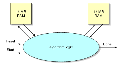
Figure 3-2 shows the algorithm view. The Algorithm Block sees two memory resources, each with independent read and write ports: up to 1M words deep and 128-bits wide per bank (up to 16 MB total per port per bank). It also sees a set of control and status flags on its Core Services Interface. Not shown in the diagram are the debug register outputs and algorithm defined memory-mapped register (MMR) inputs. Details are provided in the “Algorithm Design Details”.
This section highlights the services provided by the Core Services Block of the RASC FPGA. These features include:
Scalable System Port (SSP) Implementation: physical interface and protocol
Global Clock Generation and Control
Two sets of independent read and write ports to each of the two random access memories (SRAMs)
Single-step and multi-step control of the Algorithm Logic
Independent direct memory access (DMA) engines for read and write data
Peer Input/Output (PIO) access to algorithm's Debug port and algorithm defined registers
Control and Status registers
Host and FPGA process synchronization capabilities, including interrupts and atomic memory operations (AMOs).
The Core Services Logic provides the mechanism for application and debugger software to run the Algorithm Block in one of two modes: Normal Mode or Debug Mode. In Normal Mode, the algorithm is enabled to run and allowed to run to completion uninterrupted. In Debug Mode, the algorithm is enabled to run but forced to execute in blocks of one or more steps, allowing the user to stall the algorithm at intermediate points in the execution and query intermediate internal values. A step could be as small as one Algorithm Block clock cycle, or an adhoc size defined by Algorithm Block logic. For a description of how the Algorithm Block can use the debug mode hooks, see the “Algorithm / Core Services Block Interface ”.
This section defines the interface signals between the Algorithm Block and the Core Services Block. It covers the following topics:
The Algorithm Block (top level is alg_block_top.v/.vhd) has three groups of interface signals to the Core Services Logic.
General Algorithm Control Interface
External Memory Interface
Debug Port and Optional Algorithm Defined Registers (Algorithm-defined memory mapped space)
The associated interface signals for all three interfaces are shown in Figure 3-3, and are discussed in detail in the following sections. Not all external memory port signals are shown; only the signals for SRAM Bank 0 are included. The signals for SRAM Bank 1 are identical to those for Bank 0.

The General Algorithm Control Interface provides the algorithm with a clock, and provides reset, triggering, and stepping control. The signals on this interface are listed below. In/out is with respect to the Algorithm Block.
Table 3-1. General Algorithm Control Interface
Signal Name | in/out | Functional Description |
|---|---|---|
clk | input | 50/66/100/200 MHz gated clock, synchronous and phase-aligned to the core_clk used in the Algorithm Block. The clock frequency is determined by a macro defined at synthesis of the FPGA bitstream. The clock is driven on global clock buffers for low skew routing. |
alg_rst | input | Reset the algorithm logic. The algorithm logic is always put into reset for 4 clock cycles before triggering it to execute. Active high. |
step_flag | output | Step boundary indicator flag. For every clock cycle that step_flag is asserted, it signals to Core Services that one step has been completed. The Core Services Logic ignores this signal when the algorithm is not run in debug mode. |
alg_done | output | Set when the algorithm has finished processing. This can either be set and held until the algorithm is reset or pulsed. When alg_done is asserted, clk will become inactive the following clock cycle. The signal alg_done must clear when alg_rst is asserted. |
alg_sram0_offset[9:0] | input | Used in streaming-capable algorithms; sets the base of the segment address (upper 10 bits of 20-bit quad-word address) for input or output data residing on SRAM Bank 0. For details, see “Designing an Algorithm for Streaming” . |
alg_sram1_offset[9:0] | input | Used in streaming-capable algorithms; sets the base of the segment address (upper 10 bits of 20-bit quad-word address) for input or output data residing on SRAM Bank 1. For details, see “Designing an Algorithm for Streaming” . |
The External Memory Interface provides the algorithm with a simple interface to the read and write ports of two banks of SRAMs connected to the FPGA. Each SRAM bank provides read and write access of 16 bytes per clock cycle. The External Memory Controller encapsulates the physical layer to the SRAMs and arbitration between the other Core Services processes that can access the SRAM (DMA engines, PIO engine).
Each SRAM bank is independent from the other, and each direction (read/write) is independent, so a total of two writes and two reads can be performed simultaneously to different addresses. It is possible for the Algorithm Block to be operating on one SRAM while a DMA engine operates on another. It is also possible to have the Algorithm Logic write to a SRAM while a DMA engine (or PIO controller) reads from the same SRAM.
Access to the SRAM ports by the Algorithm Block is specified by macros defined at the synthesis of the FPGA bitstream.
The two write ports and two read ports accessible to the Algorithm Block are detailed in the tables below. In/out is with respect to the Core Services Logic. Only the signals for SRAM Bank 0 are shown. Those for SRAM Bank 1 are identical.
Table 3-2. External SRAM Bank 0 Write Interface
Signal Name | In/Out | Functional Description |
|---|---|---|
wr_addr_sram0[19:0] | output | SRAM address for an Algorithm write. This address selects a quad-word (128-bit) value. Each SRAM bank is up to 16MB, or 1M quad-words. |
wr_data_sram0[127:0] | output | 128-bit write data. |
wr_be_sram0[15:0] | output | Active high byte enables for 128-bit write data. |
wr_dvld_sram0 | output | Command to generate a write request to SRAM Bank 0, with the address, data, and byte enables specified. |
Table 3-3. External SRAM Bank 0 Read Interface
Signal Name | In/Out | Functional Description |
|---|---|---|
rd_addr_sram0[19:0] | output | SRAM address for an Algorithm Block read. This address selects a quad-word (128-bit) value. Each SRAM bank is up to 16MB, or 1M quad-words |
rd_cmd_vld_sram0 | output | Read Request Valid - command to generate a read request to SRAM Bank 0 with the address specified. |
rd_data_sram0[127:0] | input | 128-bit read data. |
rd_dvld_sram0 | input | Signals that the read data is valid. |
The Algorithm Block makes its internal signals visible to the GNU debugger software by connecting them to one or more debug output signals. The Algorithm Block can tie any internal signal or group of signals up to sixty-four, 64-bit debug outputs.
Table 3-4. Debug Port Interface
Signal Name | In/Out | Functional Description |
|---|---|---|
debug0[63:0] | output | Debug signal 0, drives host memory-mapped debug register address 0. |
debug1[63:0] | output | Debug signal 1, drives host memory-mapped debug register address 1. |
debugN[63:0] | output | Debug signal N, drives host memory-mapped debug register address N (N = {0-63}). |
debug63[63:0] | output | Debug signal 63, drives host memory-mapped debug register address 63. |
In all provided examples, the algorithm designer is required to dedicate debug register 0 to indicate the algorithm identification number and revision number.
Table 3-5. Debug Register 0 Fields Used in Sample Algorithms
Bits | Access | Reset Value | Field Name |
|---|---|---|---|
31:0 | RO | Tied | Algorithm Revision Number |
63:32 | RO | Tied | Algorithm Identification Number |
There are eight 64-bit wide software-write / hardware-read control registers with a signal indicating whether reset should be used on these registers or not. When not in use, the Algorithm Block should tie all outputs to either one or zero.
The signals on this interface include the current register values from the Core Services Block, the desired reset values from the Algorithm The use of these additional control registers is determined by algorithm needs. One suggested use for them is to pass small parameters to the algorithm that can change for each run.
Table 3-6. Optional Algorithm Defined Registers
Signal Name | In/Out | Functional Description |
|---|---|---|
alg_def_reg0 [63:0] | input | Current value of Algorithm Defined Register 0 |
alg_def_reg1 [63:0] | input | Current value of Algorithm Defined Register 1 |
alg_def_reg2 [63:0] | input | Current value of Algorithm Defined Register 2 |
alg_def_reg3 [63:0] | input | Current value of Algorithm Defined Register 3 |
alg_def_reg4 [63:0] | input | Current value of Algorithm Defined Register 4 |
alg_def_reg5 [63:0] | input | Current value of Algorithm Defined Register 5 |
alg_def_reg6 [63:0] | input | Current value of Algorithm Defined Register 6 |
alg_def_reg7 [63:0] | input | Current value of Algorithm Defined Register 7 |
alg_def_reg_rst_en | output | Enables / disables reset function of the Algorithm Defined Registers (active high). This signal should be tied high or low. When alg_def_reg_rst_en=1, all Algorithm Defined Registers will be reset to the specified reset values on core_rst (not alg_rst). When alg_def_reg_rst_en=0, reset will not affect the values of the Algorithm Defined Registers. |
alg_def_reg0_rst_val[63:0] | output | Reset value to use for Algorithm Defined Register 0 |
alg_def_reg1_rst_val[63:0] | output | Reset value to use for Algorithm Defined Register 1 |
alg_def_reg2_rst_val[63:0] | output | Reset value to use for Algorithm Defined Register 2 |
alg_def_reg3_rst_val[63:0] | output | Reset value to use for Algorithm Defined Register 3 |
alg_def_reg4_rst_val[63:0] | output | Reset value to use for Algorithm Defined Register 4 |
alg_def_reg5_rst_val[63:0] | output | Reset value to use for Algorithm Defined Register 5 |
alg_def_reg6_rst_val[63:0] | output | Reset value to use for Algorithm Defined Register 6 |
alg_def_reg7_rst_val[63:0] | output | Reset value to use for Algorithm Defined Register 7 |
This section provides information that the algorithm designer needs to implement the hardware accelerated algorithm within the FPGA and the Core Services Block framework. It covers the following topics:
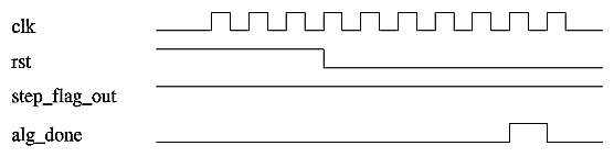
This section covers the general algorithm control sequence during a normal algorithm run (a run without breakpoints). Figure 3-4 illustrates such a sequence. The algorithm clock begins to toggle and the algorithm is put into reset for 4 algorithm clock cycles before triggering a new iteration of the algorithm.
When the algorithm is done, it should pulse its alg_done output. Once asserted, one more algorithm clock cycle will be generated. At this point, the algorithm is done and no further algorithm clock pulses will be generated for this iteration. The user can then probe the final internal Algorithm Block signals. The next time the algorithm is triggered by software, the reset sequence will start all over again. When there are no breakpoints, the activity of the step_flag signal is ignored. This particular example holds step_flag high, the method for clock based stepping.
An overview of the hardware algorithm design steps is presented in Figure 3-5. The shaded steps are covered in this section.

The RASC FPGA gives the algorithm access to two banks of up to 16MB SRAM. This section discusses the considerations for algorithm designers when deciding how to distribute input operands and parameters and output results among the available SRAM banks.
The primary recommendation for data distribution is to organize algorithm inputs and outputs on separate SRAM banks. In other words, if bank 0 is used for input data, it should not also be used for output data and vice versa (by splitting the SRAM into two logical halves, for example). The motivation for this guideline comes from the fact that when an algorithm accesses a particular bank's read or write port, it blocks access to the DMA engine that wants to unload finished results or load new operands.
To avoid multiple arbitration cycles that add to read and write latency, the algorithm is automatically given access to the ports while the algorithm is active.
In order for the hardware accelerated algorithm to run efficiently on large data sets, it is recommended to overlap data loading and unloading with algorithm execution. To do this successfully, the algorithm designer needs to start with an SRAM layout of algorithm operands and results that allows each bank to be simultaneously accessed by the Algorithm for one direction (read or write) and a DMA engine for the other direction (write or read).
The Algorithm can implement two different forms of Debug Mode, based on convenience or the desired granularity of step size: clock cycle based stepping or variable (ad hoc) stepping. The differences between the two determine the step size, or how long the algorithm will run when triggered to step once. There are also implementation differences for the step size variants. Currently, only one type of debug mode is supported at a time.
Clock cycle based stepping means that the step size is one clk cycle. This method is easily implemented in RTL-based algorithms by tying the step_flag output to one (logic high). The step counter used by the debugger is 16 bits, so the maximum number of clock cycles that can be stepped in one debugger command is 2^16-1 = 65,535.
Note that since the Algorithm Block cannot detect when clk has stopped, the effect of stepping is transparent to the Algorithm Block.
An example of this mode is shown in Figure 3-6.
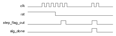
Another approach for implementing debugging is to assert step_flag at points of interest rather than every clock cycle, which makes the step size a variable number of clock cycles. One example of this method would be to use step_flag as an output of the last state of the FSM. Another example would be for the user to put in a “trigger” for when an internal counter or state machine reaches a specific value (with an indeterminate number of clock cycle steps in between). In this case, step_flag is tied to the trigger so that the algorithm can break at a designated point.
The ad hoc nature of this approach requires the Algorithm to define and notify Core Services of step boundaries with the step_flag signal. The clk signal will not stop toggling during the same clock cycle that the step_flag signal is asserted; it will turn off on the following clock cycle. See the timing diagram in Figure 3-7.
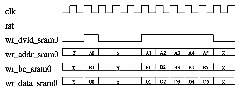
The process of using a write port involves the following step (example given for SRAM0 alone):
When the address, data and byte enables are valid for a write, assert wr_dvld_sram0 (reoccurring phase)
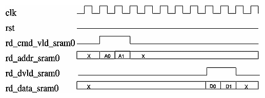
Figure 3-8 shows single and back-to-back write commands.
The process of using a read port involves the following steps (example given for SRAM0 alone):
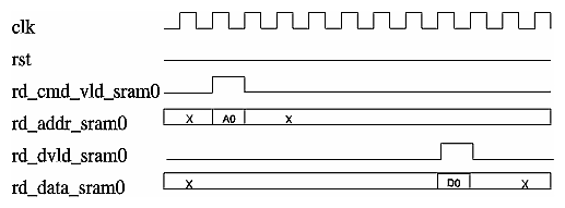
When the address is valid for a read, assert rd_cmd_vld_sram0 (reoccurring phase). This step can be repeated while waiting for data (back-to-back burst reads). The Algorithm can issue one quad-word (16 byte) read command every clk cycle per bank.
The read data will return on the bus rd_data_sram0[127:0] several clock cycles later in the order it was requested (rd_dvld_sram0 indicates that the read data is valid). The observed read latency from the Algorithm's perspective will vary based the clock period ratio between alg_clk and core_clk. Read latency is nominally 10 core_clk cycles; burst read commands are recommended for optimal read performance.
The algorithm should use the provided read data valid signal to determine when read data is valid and not attempt to count data cycles for expected latency.
Many applications targeted for hardware acceleration have large input and output data sets that will need to be segmented to fit subsets into the RASC-brick's external SRAM banks at any given time (a total of 32MB are available). Certain applications have large input data sets that have the same processing performed on subsets and only require that new input data be available in order to maintain continuous processing. These requirements bring up the notion of streaming a large data set through an algorithm. Streaming data suggests a continuous and parallel flow of data to and from the algorithm. Streaming is to sequentially load data, execute, and unload a block of data in a loop one at a time.
In order for the hardware accelerated algorithm to run efficiently on large data sets, it is recommended to overlap data loading and unloading with algorithm execution. To do this successfully, start with an SRAM layout of algorithm operands and results that complies with the recommendations for memory distribution. The input and output data needs to be segmented into at least two segments per SRAM bank so that the Algorithm Block can execute on one segment while the next data segment is loaded by the Read DMA Engine and the previous output data segment is unloaded by the Write DMA Engine (ping-pong buffer effect). The SRAM bank can be segmented into any number of segments, as the algorithm and application designers best see fit.
| Note: The term streaming as used in this section differs from the conventional definition of streaming. |
algorithm iteration
One run of the algorithm; the operation that the algorithm performs between the time alg_rst is deasserted until the alg_done flag is asserted. Successive iterations require software to retrigger the algorithm.
segment / segment size
The amount of memory needed on a particular SRAM bank for an algorithm iteration, round up to the nearest power of 2. One segment could include multiple input operands or multiple output operands, with spaces of unused memory within the segment if desired. A segment does not include fixed parameters that are applied to multiple algorithm iterations.
Streaming a segment must be at most 1/2 of the SRAM bank's size, or 8MB. The minimum segment size is 16KB (but not all 16KB need to be used). Different SRAM banks can have different segment sizes according to the sizes and number of operands / results that reside on a particular SRAM bank.
alg_sram0_offset[9:0] and alg_sram1_offset[9:0]
Inputs to the Algorithm Block that specify for each SRAM the starting address of the current data segment. When used, these inputs get mapped to the Algorithm Block's SRAM address bits [19:10] (128-bit word aligned address). The actual number of bits that are used for the mapping is determined by the segment size. If the segment size is 16KB, all 10 bits are mapped to SRAM address bits [19:10]. If the segment size is 512 KB, only bits [9:5] are mapped to SRAM address bits [19:15]. If the segment size is 16MB, only bit [9] is mapped to SRAM address bit [19].
In order to support streaming, an algorithm should allow the upper bit(s) of its read and write SRAM addresses be programmable variable via the sram*_offset inputs. The offset inputs come from an internal FPGA register within the Core Services Block, accessible by the software layer. The offset inputs are 10 bits each, and can map to bits [19:10] of the corresponding SRAM address. Only the bits that correspond to the segment offset are used for a particular algorithm/application. For example, if the segment size is 32 KB, which leads to 512 segments in the 16MB bank, only the upper 9 of the 10 offset bits are used. Example Register Transfer Level (RTL) code for this configuration is shown below:
reg [8:0] rd_segment_addr_sram0;
reg [10:0] rd_laddr_sram0;
wire [19:0] rd_addr_sram0;

// Read pointer
always @(posedge clk)
begin
	 	 // Fixed upper address bits [19:11] per iteration
	 if (rst) rd_segment_addr_sram0 <= alg_sram0_offset[9:1];

// Counter for lower address bits [10:0]
	 	if (rst)
	 	 	 rd_laddr_sram0 <= 11'h000;
else if (rd_advance_en)
	 	 	 rd_laddr_sram0 <= rd_addr_sram0 + 1'b1;
end

assign rd_addr_sram0 = {rd_segment_addr_sram0, rd_laddr_sram0};
|
The algorithm must define a legal segment size between the minimum and maximum allowable sizes, and only operate on and generate one segment worth of data per iteration.
Special extractor directives are required to pass information about the algorithm's data layout and streaming capabilities to the software layer. The software layer requires a declaration of the input and output data arrays on each SRAM bank, with attributes size, type, and buffer-ability defined. The declarations are provided as extractor directives, or comments in the Verilog or VHDL source code. The following example comments are used to declare two 16KB input data arrays located on SRAM 0, and one non-streaming input parameter array, also located on SRAM 0:
##Array name ## # of elements in array ## Bit width of element ## SRAM location ## Byte offset (within given SRAM) ## Direction ## Type ## Stream flag // extractor SRAM:input_a 2048 64 sram[0] 0x000000 in unsigned stream // extractor SRAM:input_b 2048 64 sram[0] 0x004000 in unsigned stream // extractor SRAM:param_i 512 64 sram[0] 0xffc000 in unsigned fixed |
For arrays that are defined as buffered, the byte offset provided in the extractor comments is used to establish the data placement within a particular segment. In the declaration, the byte offset is given at the lowest segment address. For fixed arrays, the byte offset is the absolute placement of the data within the SRAM.
Further details on extractor comments can be found in Chapter 5, “RASC Algorithm FPGA Implementation Guide”
Software uses configuration information derived from extractor directives to move the current active segment on each run of the algorithm. Software changes the values of sram0_offset[9:0] and sram1_offset[9:0] and for each run of the algorithm and similarly moves the DMA engines' input and output memory regions based on the current active segment.
This section describes the ways that variable parameters can get passed to the algorithm. For the purposes of this document, a parameter is distinguished from the general input data in that it can be fixed over multiple runs of the algorithm and does not require reloading. It is assumed that input data changes more often than parameters.
The method used to pass variable parameters depends on the size and number of the required parameters. For a small number of 1-8 byte-sized parameters, the Algorithm Block can associate parameters with up to eight Algorithm Defined Registers. The Algorithm Defined Registers are eight optional registers that exist within the SSP memory mapped register region whose current values are inputs to the Algorithm Block (alg_def_reg0[63:0] - alg_def_reg7[63:0]). The Algorithm Block can assign reset (default) values for the parameters by tying the output signals alg_def_reg0_rst_val[63:0] - alg_def_reg7_rst_val[63:0], and allow the host application to change them. The algorithm can also use the alg_def_reg_rst_en signal to select whether there should be a reset value, or if the parameter should be unaffected by reset.
One example is shown here is, as follows:
always @(posedge clk) begin match_val1 <= alg_def_reg0[15:0]; match_val2 <= alg_def_reg0[31:16]; end |
The algorithm passes information about the mapping of parameters to Algorithm Defined Registers to the software Abstraction Layer by way of the algorithm configuration file. The configuration file and its creation is discussed in detail in Chapter 5, “RASC Algorithm FPGA Implementation Guide”
To summarize here, comments about the parameters are added to the algorithm source code, similar to synthesis directives. Software needs to know what the parameter's descriptor is, how many bits it comprises, the data type of the parameter, and which Algorithm Defined Register it is associated with. An extractor tool parses these comments and builds up a table of algorithm specific information for use by the Abstraction Layer. Therefore, in order for these parameters to be recognized by the Abstraction Layer and used by the host application, extractor directives need to be added to the source code to indicate parameter mapping.
A simple example is provided below. In this example, the parameter match_val is 32-bits wide, unsigned, and mapped to alg_def_reg0, bits [63:32].
// extractor REG_IN:<parameter_name> <bit width> <type:signed/unsigned> alg_def_reg[<reg_num>][<bit range>] // extractor REG_IN:match_val 32 u alg_def_reg[0][63:32] |
When an algorithm requires larger fixed parameters, portions of the SRAM banks can be used to hold the parameter data. This portion of the SRAM needs to be reserved for parameter data and kept unused by input data, so parameters need to be considered in the initial memory allocation decisions. Just as with small parameters, the mapping of parameter data to SRAM addresses is specified with extractor comments. The template and an example is provided below; further details are in the “Adding Extractor Directives to the Source Code” in Chapter 5. In the provided example, a 1024-element parameter matrix (8KB) is mapped to the upper 8KB of SRAM0, which starts at address 0xFFE000. The type is unsigned and the array is fixed, which denotes that it is a parameter array and not as variable as an input data array (the other option is “stream”).
// extractor SRAM:<parameter array name> <number of elements in array> <bit width of elements> <sram bank> <offset byte address into sram> in <data type of array> fixed // extractor SRAM:param_matrix0 1024 64 sram[0] 0xFFE000 in u fixed |
Another use of declaring a fixed array in one of the SRAMs could be for a dedicated scratch pad space. The only drawback to using SRAM memory for scratch pad space is that an algorithm normally writes and then reads back scratch pad data. This usage model violates the streaming rule requiring an algorithm to dedicating each SRAM bank for either inputs or outputs. If you have a free SRAM bank that you do not need for inputs or outputs, this violation can be avoided and the streaming model can be maintained. If you have a free SRAM that is not being used for anything else, then you do not even have to add an extractor directive. An extractor directive is necessary if the SRAM bank is being used for other purposes so that software does not overwrite your scratch pad space. An extractor directive is also necessary to be able to access the scratch pad space from the debugger (reads and writes), so in general, an extractor directive is recommended.
Note that if you violate the streaming model for SRAM direction allocation, data will not be corrupted but the benefit of streaming will not occur because data transfer and algorithm execution cannot be overlapped. A template and an example is provided below for writing an extractor comment for a scratch pad space.
// extractor SRAM:<scratch_pad_array_name>
                  <number of elements in array>
                  <bit width of elements>
                  <sram bank>
                  <offset byte address into sram>
                  inout
                  <data type of array>
                  <signed / unsigned>
                  fixed

// extractor SRAM:scratch1 1024 64 sram[2] 0x000000 inout u fixed
|
These guidelines are suggestions for achieving 200 MHz timing, when possible (not including floating point operations or use of multipliers).
Flop all outputs of the algorithm block, especially critical outputs, such as step_flag.
Flop and replicate the rst input if needed to distribute it as a high fanout signal.
Flop the inputs rd_dvld_sram0 and rd_data_sram0 before performing combinatorial logic on the data or data valid signals.
The general rule to abide by when trying to code a design that passes timing at 200 MHz is this: do not give PAR (the place and route tool) any tough decisions on placement where it would be difficult to find a good location. If a critical signal loads logic in multiple blocks, replicate it so that PAR does not have to try to optimize placement of the driving flop relative to the various loading blocks. You may have to add synthesis directives to prevent the synthesis tool from “optimizing out” your manually replicated flops. As far as possible, do not have a flop drive combinational logic in one block that then loads additional combinational logic in another block (such as Core Services), unless they can be physically grouped to adjacent locations, or in the worst case, minimize the total number of logic levels.
This section shows how to make signals internal to the Algorithm Block viewable by the FPGA-enabled GNU Debugger (GDB) software. The Algorithm Block has 64 debugger output ports, each 64-bits wide. In order to make internal signals visible, the algorithm code should connect signals of interest to these outputs ports. To ease the timing issues on paths coming from the Algorithm Block, it is suggested to feed reregistered outputs to the debug outputs. Several examples are shown below:
assign debug0 = 64'h0000_000c_0000_0003; //[63:32] alg#, [31:0] rev# |
In the above example, the outputs are tied, so it is not important to register the outputs.
always @(posedge clk)
	 	 	 debug1 <= {32'h0, running_pop_count};
|
Since the intermediate value running_pop_count is also loaded by internal Algorithm Block logic, it is recommended to flop debug register 1 rather than use a wire connection. This helps isolate the loads of running_pop_count and reduce the number of constraints on the place and route program.
Besides connections to the debug port, the algorithm has to contain extractor comments that will pass the debug information to the software layer. Debug outputs use the REG_OUT type of extractor comment. The extractor comment tells the software layer what the mapping will be for internal signals to the corresponding debug address location. Examples are as follows:
// extractor REG_OUT:rev_id 32 u debug_port[0][31:0] |
and
// extractor REG_OUT:running_pop_count 32 u debug_port[1][31:0] |
The general format is:
REG_OUT:<signal name> <signal bit width> <type:unsigned/signed> <debug port connection>[<bit range>] |
This section discusses additional details, including locations of the Algorithm Block in the design hierarchy, and global FPGA logic, such as clocks and resets. It covers the following topics:
Figure 3-11 shows the instance hierarchy of the RASC FPGA design. The top-of-chip is a wrapper module called acs_top. The instances in the top level include I/O buffer wrappers, clock resources wrappers, and the two major subdivisions of the logic design: acs_core, the pre-synthesized Core Services logic, and the user_space_wrapper, the top-level wrapper for the user/algorithm logic. As the algorithm application writer, you should begin the algorithm design using alg_block_top as the top level of the algorithm. The other instances within user_space_wrapper are small parts of Core Services resources that are left to be resynthesized based on their use and fanout within the algorithm logic. These include reset fanout logic and the debug port multiplexor.

The Algorithm / Core Services interface as defined in the section entitled “Algorithm / Core Services Block Interface ”, consist of the input and output signals defined for the module alg_block_top.
This section describes the clock domains within the RASC Field Programmable Gate Array (FPGA), with a focus on the algorithm clock domain used by the Algorithm Block logic. There are two major domains: core clock and algorithm clock. However, the two domains are not completely asynchronous. They may either both be 200 MHz and phase aligned, or the algorithm clock can have a 50, 66, or 100 MHz and the clocks will be phase / edge-aligned (that is, a rising edge of the algorithm clock will correspond to a rising edge of the core clock).
This section covers the following topics:
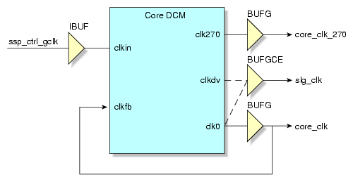
The core clock has a fixed clock rate of 200 MHz. It is the main clock used within the Core Services Block. It is derived from the input control clock on the Scalable System Port (SSP) interface. The input clock is used as the clock input to the core clock digital clock manager (DCM) module. The clk0 output of the DCM is driven onto a low-skew global clock buffer (BUFG) and from there is routed to core_clk domain registers as well as the feedback of the DCM for fine phase adjustments. In the place and route report, this clock is labelled core_clk.
The algorithm clock rate is selectable through the use of macro definitions. Speeds of 50, 66, 100, and 200 MHz can be selected. For speeds slower than 200 MHz, the DCM clock divider in the Xilinx Virtex 4 FPGA is used to create the specified clock signal. Figure 3-12 shows a block diagram of the logic used to create the clock signals.
Macro definitions are used to select between the clk0 and clkdv outputs of the DCM to drive the BUFGCE clock buffer, which in turn drives the clk signal in the Algorithm Block via the alg_clk signal.
The signal alg_clk_enable (not shown) generated by Core Services gates alg_clk. By gating the clock, the signal toggles only when the Algorithm Block is active. In the place and route clock report, this clock is labelled alg_clk.
When clkdv is used to drive the algorithm clock, the phase relationship between the core clock and the algorithm clock is determined by the Virtex 4 parameter CLKOUT_PHASE, which specifies the phase relationship between the DCM outputs of the same DCM. For Virtex 4 FPGAs, this parameters is specified as +/- 140 ps. Although the Xilinx timing tools do not take the CLKOUT_PHASE into account directly during analysis, an additional 140 ps has been added as input clock jitter to force the tools to correctly check paths crossing the core_clk and alg_clk domains. Any phase difference that is derived from the varying routes between the DCM outputs and the BUFG / BUFGCE elements as well as the clock tree fanouts are automatically considered by the Xilinx timing tools.
Core clock domain signals in the Core Services Block that communicate with the Algorithm Block, which is entirely in the alg_clk domain, have been designed to transition on the rising edge of alg_clk, even when alg_clk is run slower than the rate of core_clk.
Besides the core clock domain, which is equivalent to the Scalable System Port (SSP) control group domain, there are four data group clock domains within the SSP source synchronous receiver and transmitter logic. These four groups have a determined phase relationship between one another: each group is separated by a nominal 250 ps shift to reduce simultaneous switching noise on the SSP interface. In the place and route clock report, these clocks are labelled int_grp1_clk - int_grp4_clk.
The QDR-II SRAM module interfaces, a part of Core Services, uses five additional clock domains: one receive clock for each external SRAM (for a total of four, one for each physical SRAM component), and one common data transmit clock, which is a quarter clock cycle early relative to the core_clk. In the place and route clock report, these clocks are labelled bank0_sram_rcv_clk, bank1_sram_rcv_clk, bank2_sram_rcv_clk, bank3_sram_rcv_clk, and core_clk270.
This section describes the hardware resets in the RASC Field Programmable Gate Array. The primary reset input to the FPGA is the CM_RESET signal on the SSP port. It is used as both a clock reset and as the basis of a full-chip control logic reset. When used as a clock reset, it is used as an asynchronous reset to the DCMs in the design. A full-chip logic reset is generated based on the assertion of CM_RESET or the de-assertion of any of the DCM locked signals. There is a circuit in Core Services that generates a synchronous core_rst signal, synchronous to the core clock domain. This reset is used throughout the control logic in Core Services.
The Algorithm Block receives a different reset generated by the Core Services' Algorithm Controller sub-module. The Algorithm Block receives a reset that is synchronous to the algorithm clock. After a full-chip reset, the Algorithm Block's reset input will remain asserted even after core_rst is removed. When the algorithm is started by software for the first time, the algorithm reset is removed. This is to allow for debug testing of internal signals after the algorithm completes. When software restarts the algorithm for another run (by setting the ALG_GO bit in the CM_CONTROL Register), the Algorithm Block will be held in reset for a total of 4 algorithm clock cycles, and then the algorithm reset will be released to allow the Algorithm Block to execute.
To summarize: the Algorithm Block is held in reset until its first use. Each time the algorithm is triggered to execute, the Algorithm Block will be held in reset for 4 clock cycles.
This section describes the parameters to be specified by the algorithm designer in order to set the clock rate of the algorithm clock and to enable access to specific SRAM banks.
These synthesis-time parameters are specified in a Verilog include file called alg.h and are used by the top-level of design hierarchy. An example of this header file can be found in $RASC/example/alg_simple_v/alg.h.
The algorithm clock rate can be set at 50, 66, 100, or 200 MHz.
The following is a portion from the above example include file that selects the clock speed. This shows the four macros used to specify an algorithm clock speed.
//////////////////////////////////////////// // Specify clock speed of algorithm // //////////////////////////////////////////// // Only one of the below four should be uncommented // For 200 MHz `define alg_clk_5ns // For 100 MHz // `define alg_clk_10ns // For 66 MHz // `define alg_clk_15ns // For 50 MHz // `define alg_clk_20ns |
One and only one of the above four macros must be defined. Here the macro to set the algorithm clock rate to 200 MHz is defined and uncommented whereas the other macros are left undefined.
In order for the Algorithm Block to have access to a given SRAM port, the corresponding macro must be defined in alg.h.
The following portion from the include file enables access to SRAM ports.
//////////////////////////////////////////// // Specify SRAM ports for algorithm use // //////////////////////////////////////////// `define alg_uses_sram0_rd //`define alg_uses_sram0_wr //`define alg_uses_sram1_rd `define alg_uses_sram1_wr |
All, some, or none of these macros can be defined. In this example, the read port for SRAM bank 0 and the write port for SRAM bank 1 are enabled, while the write port for SRAM bank 0 and the read port for SRAM bank 1 cannot be used by the Algorithm Block.
If the algorithm is to buffer a large data set, the macros for the read port of one SRAM bank and the write port for the other must be undefined. Otherwise, ports will be inaccessible to the DMA engines while the Algorithm Block is active, and therefore, DMA and the Algorithm Block will not be able to operate concurrently.
This section provides a reference on how to simulate the Algorithm using the provided SSP Stub, sample test bench, and VCS simulator. It covers the following topics:
The Sample Test Bench (also called sample_tb) is a basic simulation environment for users to do sandbox testing of their algorithm code. The Sample Test Bench is provided as an optional intermediate step between writing an algorithm and loading the algorithm RASC hardware. It is intended to help insure that the algorithm will function on a basic level (e.g. a single algorithm iteration) prior to debugging a bitstream in hardware.
T he sample test bench is designed for use with VCS. For use with other simulators, the user should modify the sample test bench along with associated scripts and makefiles.
A primary component of the sample test bench, the SSP Stub, consists predominantly of Verilog modules, although it also includes PLI calls to functions written in C code. The stub is instantiated in a sample Verilog test bench along with the Algorithm FPGA. The files for this test bench are in the directory, $RASC/dv/sample_tb/. In this directory you will find the following Verilog modules and other files:
top.v: The top level of the sample test bench containing the Algorithm FPGA design (Core Services and the user's algorithm), SSP Stub, SRAM simulation models, and clock generator.
ssp_stub.v: Top level Verilog of the SSP Stub which passes signals to and from conversion modules. More information on submodules, PLI calls, and C functions that comprise the SSP Stub can be found in the “SSP Stub User's Guide” section of this document.
init_sram0.dat, init_sram1.dat, init_sram2.dat, init_sram3.dat: These SRAM initialization files contain data which is automatically loaded into the respective SRAM simulation models at the beginning of simulation. The data is in a format which the SRAM simulation model uses (one bit of parity per byte of data is shifted in with the data). These default files can be overridden by the user on the command line at runtime.
final_sram0.dat, final_sram1.dat, final_sram2.dat, final_sram3.dat: These files contain data extracted from the respective SRAM simulation models at the end of simulation. These default files can be overridden by the user on the command line at runtime.
timescale.v: This file contains the Verilog timescale of each of the components of the SSP Stub, as well as the algorithm FPGA design files. It is required that the algorithm being simulated makes use of the same timescale as the rest of the design.
In order to use the sample test bench, your VCS environment variables should be set up as follows:
### Environment Variables for VCS ### setenv VCS_HOME <your_vcs_install_directory> setenv VCSPLIDIR $VCS_HOME/<your_vcs_pli_directory> setenv PATH $PATH\:$VCS_HOME/bin |
Compiling the sample test bench is done using the Makefile provided. In order to compile the sample testbench including the SSP Stub and the algorithm Core Services logic, an algorithm must be specified (See the following note).
| Note: The Makefile in the sample_tb directory uses the $ALG_DIR environment variable. This defaults to $RASC/examples though it can be modified by the user. The design files of the algorithm you specify must be in a directory under the $ALG_DIR path. |
The algorithm you are building is specified on the command line. To compile the design with your algorithm, change directory to $RASC/dv/sample_tb and enter:
% make ALG=<your_algorithm> |
where <your_algorithm> is the directory name where the algorithm design files are. When no algorithm is specified, the default is ALG=alg_simple_v.
To remove older compiled copies of the testbench, type:
% make clean |
To run a diagnostic on your algorithm, call the Makefile in the sample_tb directory using the “run” target and specifying which diag to run. The following is the usage and options of the “run” target:
% make run DIAG=diag_filename ALG=your_agorithm SRAM0_IN=sram0_input_file SRAM1_IN=sram1_input_file SRAM2_IN=sram2_input_file SRAM3_IN=sram3_input_file SRAM0_OUT=sram0_output_file SRAM1_OUT=sram1_output_file SRAM2_OUT=sram2_output_file SRAM3_OUT=sram3_output_file |
The diag_file specifies the diagnostic to be run and should be relative to the current directory. Again, the algorithm must be specified using the ALG=your_algorithm command line option. If none is specified, the runtime command uses same default as above (ALG=alg_simple_v). Specifying ALG this way allows the user to reuse the same diagnostic for multiple algorithms. The contents of each SRAM at the end of simulation will be dumped into .dat files that can be user-specified. If they are not specified, they default to:
init_sram0_good_parity.dat init_sram1_good_parity.dat init_sram2_good_parity.dat init_sram3_good_parity.dat final_sram0.dat final_sram1.dat final_sram2.dat final_sram3.dat |
Note that there are four input and four output SRAM data files while the design is implemented for two logical SRAMs. Each of the logical SRAMs is implemented as two separate physical SRAMs in the sample testbench. The sram0* and sram1* files correspond to the first logical SRAM while sram2* and sram3* correspond to the second logical SRAM.
By specifying the SRAM input and output files the user can skip the DMA process for quick verification of the algorithm. This shortens the diagnostic run time, makes for less complex diagnostics, and allows the user to ignore core services as it has already been verified by SGI. The option of utilizing the DMA engines in simulation is included for completeness but should not be necessary for typical algorithm verification.
As the diagnostic runs, it will output status to the screen and to an output file named <diag_filename>.<your_algorithm>.run.log. When the stub receives an unexpected packet, it will output the following information in order: the command for the next expected packet, SSP fields of the expected packet, the command translation (if one exists) for the received packet, and the SSP fields of the received packet. This log file will appear in the same directory in which that the diagnostic is located.
Table 3-7 shows a summary of the algorithms, diagnostics, and commands provided with the sample testbench.
Table 3-7. Sample Testbench Algorithms and Commands
Algorithm Name | Diagnostic | Compile and Run Commands |
|---|---|---|
alg_simple_v | diags/alg_simple_v | make ALG=alg_simple_v make run DIAG=diags/alg_simple_v ALG=alg_simple_v |
alg_data_flow_v | diags/alg_data_flow_v | make ALG=alg_data_flow_v make run DIAG=diags/alg_data_flow_v ALG=alg_data_flow_v |
Each time a diagnostic is run, a file named vcdplus.vpd is generated in the sample_tb directory. This file can be input to Virsim for viewing the waveform. Since this file is generally large, it is overwritten for each diagnostic run. To save the waveform for a given diagnostic, copy the corresponding vcdplus.vpd file to a new name.
To view the waveform saved in the vcdplus.vpd file, use the following command:
% vcs -RPP vcdplus.vpd |
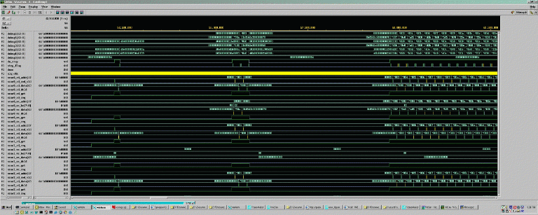
A sample configuration file sample_tb/basic.cfg is provided in the for use when viewing waveforms in Virsim. It contains a limited number of relevant signals on the SSP interface, SRAM interfaces, and inside the design. Figure 3-13 shows a sample vcdplus.vpd waveform in Virsim.
The SSP Stub retrieves instructions through a text input file, the diagnostic. The SSP Stub parses this file at each semicolon to extract commands that the Stub executes. Many of the allowed commands in a diagnostic correspond to SSP packet types. There are other commands that the SSP Stub supports for diagnostic writing and debugging. The primary components of the diagnostic file are: packet commands, debugging commands, and comments.
It is important to note that most SSP packets come in pairs: a request and a response. For these types of packets, the request command and response command must be listed sequentially in a diagnostic. This method of keeping requests and response paired is used by the stub to associate request and response packets with the corresponding transaction number (TNUM). For more information on SSP packet types, see the Scalable System Port Specification. Also, when running the DMA engines, all transactions related to that sequence of events should be grouped together. See Appendix B, “SSP Stub User's Guide” for more details on diagnostic writing and using the SSP stub.
The code listed below comprises a diagnostic that exercises the basic functionality of the algorithm FPGA outlined in the following steps:
Initializes the algorithm FPGA Core Services (primarily MMR Writes)
Executes DMA Reads to send data to the FPGA (stored in SRAM)
Starts the Algorithm (d = a & b | c) and polls the memory mapped registers (MMRs) to see when the Algorithm is done
Executes DMA Writes to retrieve the Algorithm's results
Checks the error status in the MMRs to verify that no errors were flagged.
The example diagnostic provided below is intended as a template that may be edited to match the user's algorithm.
#######  Initialization packets.  #######
# Arm regs by setting the REARM_STAT_REGS bit in the CM_CONTROL reg
snd_wr_req ( PIO, DW, ANY, 0x00000000000020, 0x0000000600f00003 );
rcv_wr_rsp ( PIO, DW, ANY, 0 );

# Clear the CM_ERROR_STATUS register by writing all zeroes.
snd_wr_req ( PIO, DW, 3, 0x00000000000060, 0x0000000000000000 );
rcv_wr_rsp ( PIO, DW, 3, 0);

# Enable CM_ERROR_DETAIL_* regs by writing all zeroes to CM_ERROR_DETAIL_1.
snd_wr_req ( PIO, DW, ANY, 0x00000000000010, 0x0000000000000000 );
rcv_wr_rsp ( PIO, DW, ANY, 0 );

# Enable desired interrupt notification in the CM_ERROR_INTERRUPT_ENABLE
register.
snd_wr_req ( PIO, DW, 4, 0x00000000000070, 0xFFFFFFFFFFFFFFFF );
rcv_wr_rsp ( PIO, DW, 4, 0 );

# Set up the Interrupt Destination Register.
snd_wr_req ( PIO, DW, ANY, 0x00000000000038, 0x0000000000000000 );
rcv_wr_rsp ( PIO, DW, ANY, 0 );

print "\n\n*******Initialization finished\n\n";


#######  Configure DMA Engines and Algorithm.  #######

#######  Configure the Read DMA Engine Registers.  #######
print "\n\n*******Configure Read DMA Engine.  Tell it to fill 32 cache lines
of data.\n\n";

# RD_DMA_CTRL register.
snd_wr_req ( PIO, DW, ANY, 0x00000000000110, 0x0000000000100020 );
rcv_wr_rsp ( PIO, DW, ANY, 0 );

# RD DMA addresses.
snd_wr_req ( PIO, DW, ANY, 0x00000000000100, 0x0000000000100000 );
rcv_wr_rsp ( PIO, DW, ANY, 0 );
snd_wr_req ( PIO, DW, ANY, 0x00000000000108, 0x0000000000000000 );
rcv_wr_rsp ( PIO, DW, ANY, 0 );

# RD AMO address.
snd_wr_req ( PIO, DW, ANY, 0x00000000000118, 0x0000000000000000 );
rcv_wr_rsp ( PIO, DW, ANY, 0 );

# RD_DMA_DEST_INT
snd_wr_req ( PIO, DW, ANY, 0x00000000000120, 0x0000000200002000 );
rcv_wr_rsp ( PIO, DW, ANY, 0 );


#######  Configure the Write DMA Engine Registers.  #######
print "\n\n*******Configure Write DMA Engine.\n\n";

# Write to the WR_DMA_CTRL register.
snd_wr_req ( PIO, DW, ANY, 0x00000000000210, 0x0000000000100020 );
rcv_wr_rsp ( PIO, DW, ANY, 0 );

# WR_DMA_SYS_ADDR
snd_wr_req ( PIO, DW, ANY, 0x00000000000200, 0x0000000000100000 );
rcv_wr_rsp ( PIO, DW, ANY, 0 );

# WR_DMA_LOC_ADDR
snd_wr_req ( PIO, DW, ANY, 0x00000000000208, 0x0000000000000000 );
rcv_wr_rsp ( PIO, DW, ANY, 0 );

# WR_DMA_AMO_DEST
snd_wr_req ( PIO, DW, ANY, 0x00000000000218, 0x0000000000000000 );
rcv_wr_rsp ( PIO, DW, ANY, 0 );

# WR_DMA_INT_DEST
snd_wr_req ( PIO, DW, ANY, 0x00000000000220, 0x0000000400004000 );
rcv_wr_rsp ( PIO, DW, ANY, 0 );

#######  Configure the Algorithm Registers.  #######
print "\n\n*******Configure Algorithm Registers\n\n";

snd_wr_req ( PIO, DW, ANY, 0x00000000000300, 0x0000000000000000 );
rcv_wr_rsp ( PIO, DW, ANY, 0 );

snd_wr_req ( PIO, DW, ANY, 0x00000000000308, 0x0000000600006000 );
rcv_wr_rsp ( PIO, DW, ANY, 0 );


#######  Start Read DMA Engine for Read DMA 1  #######
print "\n\n*******Start Read DMA Engine for SRAM0\n\n";

# Set Bit 36 of the CM_CONTROL Reg to 1.
snd_wr_req ( PIO, DW, ANY, 0x00000000000020, 0x0000001400f00003 );
rcv_wr_rsp ( PIO, DW, ANY, 0 );

# 1 of 32
rcv_rd_req ( MEM, FCL, ANY, 0x00000000100000 );
snd_rd_rsp ( MEM, FCL, ANY, 0, 0xDEADBEEFDEADBEEF, 0xDEADBEEFDEADBEEF,
                               0xDEADBEEFDEADBEEF, 0xDEADBEEFDEADBEEF,
                               0xDEADBEEFDEADBEEF, 0xDEADBEEFDEADBEEF,
                               0xDEADBEEFDEADBEEF, 0xDEADBEEFDEADBEEF,
                               0xDEADBEEFDEADBEEF, 0xDEADBEEFDEADBEEF,
                               0xDEADBEEFDEADBEEF, 0xDEADBEEFDEADBEEF,
                               0xDEADBEEFDEADBEEF, 0xDEADBEEFDEADBEEF,
                               0xDEADBEEFDEADBEEF, 0xDEADBEEFDEADBEEF );

# Other Read DMA Transactions omitted here

# 32 of 32
rcv_rd_req ( MEM, FCL, ANY, 0x00000000100F80 );
snd_rd_rsp ( MEM, FCL, ANY, 0, 0xDEADBEEFDEADBEEF, 0xDEADBEEFDEADBEEF,
                               0xDEADBEEFDEADBEEF, 0xDEADBEEFDEADBEEF,
                               0xDEADBEEFDEADBEEF, 0xDEADBEEFDEADBEEF,
                               0xDEADBEEFDEADBEEF, 0xDEADBEEFDEADBEEF,
                               0xDEADBEEFDEADBEEF, 0xDEADBEEFDEADBEEF,
                               0xDEADBEEFDEADBEEF, 0xDEADBEEFDEADBEEF,
                               0xDEADBEEFDEADBEEF, 0xDEADBEEFDEADBEEF,
                               0xDEADBEEFDEADBEEF, 0xDEADBEEFDEADBEEF );

print "\n\n*******Polling for DMA RD-SRAM0 done (bit 42 of CM_STATUS).\n\n";
poll (0x8, 42, 20);
print "\n\n*******Done storing data in SRAM 0.\n\n";


#######  Reconfigure DMA Engine for Read DMA 2  #######

# RD_DMA_SYS_ADDR
snd_wr_req ( PIO, DW, ANY, 0x00000000000100, 0x0000000000100000 );
rcv_wr_rsp ( PIO, DW, ANY, 0 );

# RD_DMA_LOC_ADDR
snd_wr_req ( PIO, DW, ANY, 0x00000000000108, 0x0000000000200000 );
rcv_wr_rsp ( PIO, DW, ANY, 0 );


#######  Start Read DMA Engine for Read DMA 2  #######
print "\n\n*******Start Read DMA Engine for SRAM1\n\n";

# Set Bit 36 of the CM_CONTROL Reg to 1.
snd_wr_req ( PIO, DW, ANY, 0x00000000000020, 0x0000001400f00003 );
rcv_wr_rsp ( PIO, DW, ANY, 0 );

# 1 of 32
rcv_rd_req ( MEM, FCL, ANY, 0x00000000100000 );
snd_rd_rsp ( MEM, FCL, ANY, 0, 0xF0F0F0F0F0F0F0F0, 0xF0F0F0F0F0F0F0F0,
                               0xF0F0F0F0F0F0F0F0, 0xF0F0F0F0F0F0F0F0,
                               0xF0F0F0F0F0F0F0F0, 0xF0F0F0F0F0F0F0F0,
                               0xF0F0F0F0F0F0F0F0, 0xF0F0F0F0F0F0F0F0,
                               0xF0F0F0F0F0F0F0F0, 0xF0F0F0F0F0F0F0F0,
                               0xF0F0F0F0F0F0F0F0, 0xF0F0F0F0F0F0F0F0,
                               0xF0F0F0F0F0F0F0F0, 0xF0F0F0F0F0F0F0F0,
                               0xF0F0F0F0F0F0F0F0, 0xF0F0F0F0F0F0F0F0 );

# Other Read DMA Transactions omitted here

# 32 of 32
rcv_rd_req ( MEM, FCL, ANY, 0x00000000100F80 );
snd_rd_rsp ( MEM, FCL, ANY, 0, 0xF0F0F0F0F0F0F0F0, 0xF0F0F0F0F0F0F0F0,
                               0xF0F0F0F0F0F0F0F0, 0xF0F0F0F0F0F0F0F0,
                               0xF0F0F0F0F0F0F0F0, 0xF0F0F0F0F0F0F0F0,
                               0xF0F0F0F0F0F0F0F0, 0xF0F0F0F0F0F0F0F0,
                               0xF0F0F0F0F0F0F0F0, 0xF0F0F0F0F0F0F0F0,
                               0xF0F0F0F0F0F0F0F0, 0xF0F0F0F0F0F0F0F0,
                               0xF0F0F0F0F0F0F0F0, 0xF0F0F0F0F0F0F0F0,
                               0xF0F0F0F0F0F0F0F0, 0xF0F0F0F0F0F0F0F0 );

print "\n\n*******Polling for DMA RD-SRAM1 done (bit 42 of CM_STATUS).\n\n";
poll (0x8, 42, 200);
print "\n\n*******Done storing data in SRAM 1.\n\n";


#######  Reconfigure DMA Engine for Read DMA 3  #######

# RD DMA addresses.
snd_wr_req ( PIO, DW, ANY, 0x00000000000100, 0x0000000000100000 );
rcv_wr_rsp ( PIO, DW, ANY, 0 );
snd_wr_req ( PIO, DW, ANY, 0x00000000000108, 0x0000000000400000 );
rcv_wr_rsp ( PIO, DW, ANY, 0 );


#######  Start Read DMA Engine for Read DMA 3  #######
print "\n\n*******Start Read DMA Engine for SRAM2\n\n";

# Set Bit 36 of the CM_CONTROL Reg to 1.
snd_wr_req ( PIO, DW, ANY, 0x00000000000020, 0x0000001400f00003 );
rcv_wr_rsp ( PIO, DW, ANY, 0 );

# 1 of 32
rcv_rd_req ( MEM, FCL, ANY, 0x00000000100000 );
snd_rd_rsp ( MEM, FCL, ANY, 0, 0x0C0C0C0C0C0C0C0C, 0x0C0C0C0C0C0C0C0C,
                               0x0C0C0C0C0C0C0C0C, 0x0C0C0C0C0C0C0C0C,
                               0x0C0C0C0C0C0C0C0C, 0x0C0C0C0C0C0C0C0C,
                               0x0C0C0C0C0C0C0C0C, 0x0C0C0C0C0C0C0C0C,
                               0x0C0C0C0C0C0C0C0C, 0x0C0C0C0C0C0C0C0C,
                               0x0C0C0C0C0C0C0C0C, 0x0C0C0C0C0C0C0C0C,
                               0x0C0C0C0C0C0C0C0C, 0x0C0C0C0C0C0C0C0C,
                               0x0C0C0C0C0C0C0C0C, 0x0C0C0C0C0C0C0C0C );

# Other Read DMA Transactions omitted here

# 32 of 32
rcv_rd_req ( MEM, FCL, ANY, 0x00000000100F80 );
snd_rd_rsp ( MEM, FCL, ANY, 0, 0x0C0C0C0C0C0C0C0C, 0x0C0C0C0C0C0C0C0C,
                               0x0C0C0C0C0C0C0C0C, 0x0C0C0C0C0C0C0C0C,
                               0x0C0C0C0C0C0C0C0C, 0x0C0C0C0C0C0C0C0C,
                               0x0C0C0C0C0C0C0C0C, 0x0C0C0C0C0C0C0C0C,
                               0x0C0C0C0C0C0C0C0C, 0x0C0C0C0C0C0C0C0C,
                               0x0C0C0C0C0C0C0C0C, 0x0C0C0C0C0C0C0C0C,
                               0x0C0C0C0C0C0C0C0C, 0x0C0C0C0C0C0C0C0C,
                               0x0C0C0C0C0C0C0C0C, 0x0C0C0C0C0C0C0C0C );

print "\n\n*******Polling for DMA RD-SRAM2 done (bit 42 of CM_STATUS).\n\n";
poll (0x8, 42, 200);
print "\n\n*******Done storing data in SRAM 2.\n\n";

#######  Start the Algorithm  #######

# Set bit 38 of CM Control Register to 1 to start algorithm.
snd_wr_req ( PIO, DW, ANY, 0x00000000000020, 0x0000004400f00003 );
rcv_wr_rsp ( PIO, DW, ANY, 0 );

print "\n\n*******Started Algorithm.\n\n";

# Poll for ALG_DONE bit in CM_STATUS.
poll ( 0x8, 48, 2000);
print "\n\n*******Algorithm Finished.\n\n";

#######  Start Write DMA Engine.  #######

# Set bit 37 of CM Control Register to 1 to start Write DMA Engine.
snd_wr_req ( PIO, DW, ANY, 0x00000000000020, 0x0000002400f00003 );
rcv_wr_rsp ( PIO, DW, ANY, 0 );

print "\n\n*******Started Write DMA Engine.\n\n";

# 1 of 32
rcv_wr_req ( MEM, FCL, ANY, 0x00000000100000, 0xDCACBCECDCACBCEC,0xDCACBCECDCACBCEC,
                                              0xDCACBCECDCACBCEC,0xDCACBCECDCACBCEC,
                                              0xDCACBCECDCACBCEC,0xDCACBCECDCACBCEC,
                                              0xDCACBCECDCACBCEC,0xDCACBCECDCACBCEC,
                                              0xDCACBCECDCACBCEC,0xDCACBCECDCACBCEC,
                                              0xDCACBCECDCACBCEC,0xDCACBCECDCACBCEC,
                                              0xDCACBCECDCACBCEC,0xDCACBCECDCACBCEC,
                                              0xDCACBCECDCACBCEC,0xDCACBCECDCACBCEC );
snd_wr_rsp ( MEM, FCL, ANY, 0 );

# Other Write DMA Transactions omitted here

# 32 of 32
rcv_wr_req ( MEM, FCL, ANY, 0x00000000100F80, 0xDCACBCECDCACBCEC,0xDCACBCECDCACBCEC,
                                              0xDCACBCECDCACBCEC,0xDCACBCECDCACBCEC,
                                              0xDCACBCECDCACBCEC,0xDCACBCECDCACBCEC,
                                              0xDCACBCECDCACBCEC,0xDCACBCECDCACBCEC,
                                              0xDCACBCECDCACBCEC,0xDCACBCECDCACBCEC,
                                              0xDCACBCECDCACBCEC,0xDCACBCECDCACBCEC,
                                              0xDCACBCECDCACBCEC,0xDCACBCECDCACBCEC,
                                              0xDCACBCECDCACBCEC,0xDCACBCECDCACBCEC );
snd_wr_rsp ( MEM, FCL, ANY, 0 );

print "\n\n*******Polling for DMA WR-SRAM0 done (bit 45 of CM_STATUS).\n\n";
poll (0x8, 45, 200);
print "\n\n*******Done retrieving data from SRAM 0.\n\n";

#######  Finish Up  ######

# dma_clear().  Set bits 39, 40, and 41 to 1 in CM_CONTROL.
snd_wr_req ( PIO, DW, ANY, 0x00000000000020, 0x0000038400f00003 );
rcv_wr_rsp ( PIO, DW, ANY, 0 );

# finalcheck_ccc() Check CACHE_RD_DMA_FSM.
snd_rd_req ( PIO, DW, ANY, 0x00000000000130 );
rcv_rd_rsp ( PIO, DW, ANY, 0, 0x0000000000400000 );

print "Reading the Error Status Register to insure no errors were
logged.\n";
snd_rd_req ( PIO, DW, ANY, 0x00000000000060 );
rcv_rd_rsp ( PIO, DW, ANY, 0, 0x0000000000000000 );
|
Various constants and definitions for the sample test bench are contained within the following files:
ssp_defines.h (internal stub variables)
user_const.h (user modifiable)
Table 3-8 lists the files in the sample_tb directory with their function and calls dependencies.
Table 3-8. Files in the sample_tb directory
File | Functions | Dependent On |
|---|---|---|
start_ssp.c | start_ssp() | queue_pkt.h, setup_pkt.h, send_rcv_flits.h |
send_rcv_flits.h | send_rcv_flits(), send_flit(), rcv_flit(),snd_poll(), rcv_poll(), finish_ssp() | setup_pkt.h, process_pkt.h, get_fields.h, snd_rcv_fns.h |
queue_pkt.h | queue_pkt(string), q_string_it(token, pkt_string),strtok_checked(s1, s2) | -- |
setup_pkt.h | setup_pkt(snd_rcv) | snd_rcv_fns.h |
snd_rcv_fns.h | snd_wr_req(pio_mem_n, size, tnum, addr, data, pkt), snd_rd_req(pio_mem_n, size, tnum, addr, pkt), snd_wr_rsp(pio_mem_n, size, tnum, error, pkt), snd_rd_rsp(pio_mem_n, size, tnum, error, data), snd_amo_rsp(tnum, error, pkt), inv_flush(tnum, pkt), rcv_wr_rsp(pio_mem_n, size, tnum, error, pkt), rcv_rd_rsp(pio_mem_n, size, tnum, error, data, pkt), rcv_wr_req(pio_mem_n, size, tnum, addr, data, pkt), rcv_rd_req(pio_mem_n, size, tnum, addr, pkt),rcv_amo_req(tnum, addr, data, pkt) | construct_pkt.h |
construct_pkt.h | construct_pkt(type, tnum, address, data, error, pkt, to_from_n), pkt_size(type) | make_command.h |
make_command.h | make_command(type, tnum, error, to_from_n) | -- |
get_fields.h | get_fields(type), f_string_it(token) | -- |
process_pkt.h | process_pkt(type) | -- |
The sample test bench includes utilities that help in generating and interpreting diagnostic data. To compile these files into executables, run the following command:
% gcc -c file_name -o executable name |
The utilities provided include the following:
convert_sram_to_dw.c
This program takes a standard SRAM input/output file (e.g. final_sram0.dat), and converts it to a more readable version consisting of one SGI double word (64-bits) of data per line. It assumes that the input file is made up of 36-bit words containing parity bits. This utility is helpful when trying to interpret results from the stub output files.
Use: convert_sram_to_dw input_file [output_file]
Default output file: convert_sram_to_dw_output.dat
convert_dw_to_sram_good_parity.c
This program takes a file containing one SGI double word (64-bits) of data per line, calculates parity and outputs a file that can be loaded into SRAM for simulation (36-bits of data with parity per line). It assumes the input file contains the correct number of lines to fill the SRAM. This utility is useful when you want to input specific data to an SRAM and skip the DMA process in simulation.
Use: convert_dw_to_sram_good_parity input_file [output_file]
Default output file: convert_dw_to_sram_good_parity_output.dat.
command_fields.c
This program takes an SSP command word, splits it into its SSP fields and outputs the SSP field information to the screen. The utility provides this data in the same format as the get_fields.h function in the SSP stub. This feature is potentially useful in debugging from the Virsim viewer.
Use: command_fields 32-bit_hex_value
check_alg_data_flow.c
This program uses the SRAM output file to check data against input data. It takes the data in init_sram0_good_parity.dat, removes parity, and performs a byte-sort on this data (byte-sorts each 8 byte quantity as done by alg_data_flow_v). The program compares the result to the data in the file final_sram1.dat (with parity removed). As the comparisons are done, the program prints the byte-sorted input data on the left and the results from the final data on the right. If there are differences in the data, it prints "ERROR" on the corresponding line. The program exits after it finding a finite number of errors (adjustable in the source code).
check_alg_simple.c
This file is an example of a program that uses the SRAM output data file to check data against input data. It takes the SRAM0 and SRAM1 input data in init_sram0_good_parity.dat and init_sram1_good_parity.dat and calculates the results of a A & B | C. It then compares its expected data to the data in the files final_sram2.dat and final_sram3.dat (the default output for SRAM2 and SRAM3, respectively). As it proceeds, it prints out the results of each double word result D: on the left, what it expects based on the input data, on the right, what it is seeing in the final results. If there are discrepancies in the data, it prints "ERROR" on the line in question.
The code is set to exit after it finds 64 errors, but this number can be raised or lowered easily (line 60).
A recently implemented feature of the sample test bench is the support of a limited set of rasclib calls. The intent is to allow you to compile your application code with simple simulation definitions of rasclib commands such as rasclib_algorithm_send(), rasclib_algorithm_go(), rasclib_algorithm_receive(), and so on. Using simulation, you can specify input data, start your algorithm, and verify output for a single iteration of the algorithm.
Using rasclib in simulation is suggested for testing and debugging an algorithm early in development. Simulation using rasclib has limitations that may require you to limit the complexity of your implementation while simulating. A couple of guidelines are, as follows:
Limit simulation to a single iteration of the algorithm
Limit the amount of data consumed or produced by the algorithm to around 4KB (for simulation only)
Allowing the algorithm to work on several megabytes of data is useful for implementation in real hardware but is typically unreasonable for simulation. Limiting data will help insure that simulation completes in a reasonable amount of wall clock time.
Simulating with rasclib requires the following:
The RTL of the algorithm block (alg_block_top.v) and any submodules. For simulation, this RTL should be located in the $RASC/examples/<alg_name>/ directory which should be created by the user.
User application code which calls the user's algorithm. For simulation, this is application code should be located in the $RASC/dv/sample_tb/tests/ directory which is part of the sample test bench. It is recommended, though not required that the application code be named <alg_name>.cpp as has been done for the examples provided.
The configuration file contains a description of where inputs and outputs should be located in local memory. For simulations, this configuration file should be located in the existing $RASC/dv/sample_tb/tests/ directory. For simulation, this configuration file should be named <alg_name>.cfg. Unlike the other files above, this file is not written by the user. Rather, it is generated as part of algorithm implementation. The configuration file is output from the Extractor script which is described in Appendix C, “How Extractor Works”.
Working examples of each of these files can be found in their respective locations. To simulate using rasclib, the application code must be compiled with the simulation version of the rasclib calls. A Makefile has been provided to help compile the application code correctly. To compile, ensure that the RTL, application code, and configuration file are in their respective locations. Then go to the $RASC/dv/sample_tb/tests/ directory and enter make <alg_name>. For example:
make alg_simple_v |
Or:
make alg_data_flow_v |
This compiles the application code found in this directory. The application code will compile with the simulation version of the rasclib calls that are responsible for running the simulator. The executable that is generated is named the same as the application code without the dot suffix file extension. Once this compiles cleanly, run the executable. For example:
./alg_simple_v |
Or:
./alg_data_flow_v |
This executes the application. The appropriate rasclib calls send data from the application to the simulator, compile and run the simulator, and provide the results from the simulator back to the application. For more details on simulating rasclib, SGI recommends that you try the sample algorithms and look through the sample application code provided. To compile application code from a clean state, start by executing this command:
make clean |
The final application code that runs the algorithm in hardware (non-simulation) may likely have significant functionality that differs from the application code used for debugging with the simulation version of rasclib. Below are some differences to keep in mind for porting applications written for rasclib on the 64-bit Altix platform to the simulation rasclib environment (typically a 32-bit programming environment). Note that these differences have already been incorporated into the samples provided.
Change variables of type unsigned long to type unsigned long long for simulation.
Limit the array buffer size to one algorithm run for simulation. It should match the array size in the configuration file (e.g. alg_simple_v.cfg).