This chapter describes the DVP Specifications. It contains the following sections:
Overview
Physical Characteristics
Signal Descriptions
Electrical Considerations
16-bit Luminance
Video Format Programming
Genlock DG4 to External Sources
Signal Lists
The InfiniteReality™ Digital Video Port (DVP) provides digital video data from the InfiniteReality frame buffer in raster-scan order, left-to-right, top-to-bottom, one pixel at a time, at the pixel clock rate. Pixel data is 36 bits wide (12 bits per component, RGB). Support is also provided for accessing 16-bit luminance information. (See “16-Bit Luminance” for more information.)
The DVP minimizes latency to video data. Typically, there is less than one horizontal period of latency in the video data. The exact latency depends on the particular video format and the pixel clock speed. There are three distinct “break-points”: 2.5 to 60 Mpix/sec, 60 to 120 Mpixels/sec, and 120 to 230 Mpixels/sec. The highest clock rate adds 3 pixel clocks of delay, the mid-range adds a total of 2 pixel clocks of delay, and the low range adds no delay. In all three cases, the relationship of CBLANK_{H,L} to video data is constant. (See “Timing Signals” for more information.) The latency is negligible in most applications. Digital video data on the DVP appears in the same frame as video on the analog channels.
The DVP physical interface consists of a single, 100-conductor, 110-ohm cable organized as 45 differential signal pairs. These signal pairs consist of the following:
36 RGB data pairs
2 clock pairs
5 pairs of timing signals (horizontal and vertical sync, composite blank (video active), even/odd field, and VOC_SWAP)
2 pairs of Silicon Graphics-reserved signals
There are also 7 ground connections, a receiver power indicator, and 2 signals implementing the I2C serial control channel. The DVP cable connects the digital video stream from the InfiniteReality graphics system to a video peripheral board located outside the Silicon Graphics logic cabinet in a customer-supplied chassis.
The maximum DVP cable length is 3 meters (about 10 feet). This length guarantees operation at the maximum specified data rate for the DVP interface. (For applications where the pixel clock rate is reduced, longer cable lengths may be possible but have not been characterized at this time.)
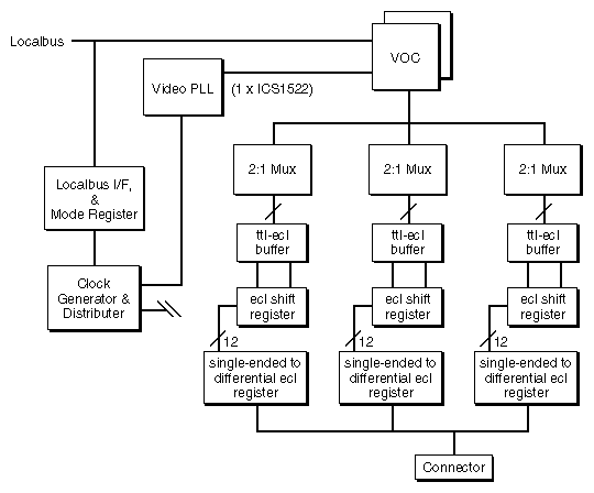
The DVP external cable plugs into a connector assembly called the DVIO1, which is located in the door of the Onyx® logic cabinet. A special flat internal cable connects the DVIO1 to a daughterboard mounted on the DG4 video display board. The daughterboard is called the DVP board. This card implements a user-programmable digital video channel similar to the other analog video channels of the InfiniteReality graphics subsystem. Figure 1-1 shows the block diagram of the DVP daughterboard.
The other end of the external DVP cable plugs into customer-designed equipment, which complies with this specification.
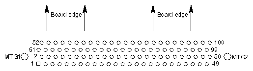
The receiver connector must be mechanically and electrically compatible with the following connector: 3M part number 102A0-5242VC. There should be no built-in EMI filtering because of the deleterious effect it would have on electrical performance. (See Figure 1-2 for the component-side connector footprint.)
 | Note: The connector pin-out depends on which end of the cable it is connected. (See Table 1-1 and Table 1-2 for the transmit and receive pinouts.) |
The DVP interface features differential, 5-volt positive-ECL (5V-PECL) signalling. This document uses the UNIX® syntactic convention of “curly braces” to show alternatives for the signal polarity. This convention allows a single name to refer to both of the signals in the differential pair, yet makes it obvious that there are two signals. (In actual schematics, each differential pair signal has its own name with the polarity specified and the curly braces omitted. For example, this document might describe a differential pair as FOO_{H,L}, whereas actual schematics would show the pair of signals as FOO_H and FOO_L.)
There are 72 video data signals, which comprise 36 differential signal pairs. These are split into three color components of 12 bits each: (RED_OUT_{H,L}[11:0], GREEN_OUT_{H,L}[11:0], BLUE_OUT_{H,L}[11:0]). The InfiniteReality DVP interface does not include the Alpha channel.
This document uses the following video data signal naming convention: ColorComponentName_OUT_SignalPolarity[SignificantBit]. The last digit of the signal name indicates the binary significance of the digital color component. For example, the most significant bit of the positive-logic version green component is GREEN_OUT_H[11].
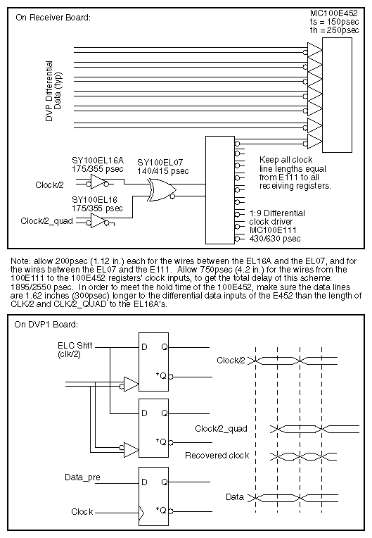
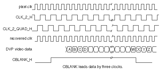
To control in-flight skew between clock and data caused by nonuniform group delay in the cable, it is important to carefully match the spectral characteristics of the clocks to the data transmitted on the DVP interface. This is accomplished by transmitting an in-phase and a quadrature-phase version of the pixel clock, divided by 2. (See Figure 1-4 for Silicon Graphics recommendations for recovering a full-speed pixel clock on the receiver. See Figure 1-5 for Timing Diagram information.)
CBLANK_{H,L}, CSYNC_{H,L}, VSYNC_{H,L}, FIELD_{H,L} indicate the structure of the video raster being transmitted by the DVP interface. Except for CBLANK_{H,L} and FIELD_{H,L}, these signals are user-programmable via the Video Format Compiler. (For more information, see the InfiniteReality Video Format Compiler Programming Guide, part number 007-3402-001). CBLANK serves as an indicator of active video. It has a fixed, non-programmable, 3-pixel clock skew with respect to video. CBLANK will transition active/inactive 3 pixel clocks (3 edges of CLK_2_QUAD) before video data. The skew allows for easy implementation of control circuits in the receiver. FIELD_{H,L} indicates the field that is currently being transmitted. For non-interlaced video formats, FIELD_H is always inactive (low). For interlaced formats, FIELD_H is always active (high) throughout the second field of the frame.
The VOC_SWAP signal indicates the first frame of video that occurs after the framebuffer memory has been swapped. This is the default semantics of this signal. VOC_SWAP is actually a catch-all signal. It may be statically programmed to send any one of the following 6 video signals:
line-start
field-start
frame-start
tri-sync (useful for generating analog HDTV signals)
vdrc-enable (the window during which the VOC is allowed to request video data from the framebuffer. VOC_SWAP is actually vdrc_en, conditioned with a latched version of the framebuffer swap signal).
VOC_SWAP can also be programmed to be continuously HI or LOW.
For more information, contact Silicon Graphics technical support or your local service provider.
These signals are reserved for future development of the DVP interface. The current implementation always asserts these two signal pairs as LOW.
The DVP interface uses differential, 5-volt positive-ECL (5V-PECL) signalling, which provides speed and the ability to correctly terminate transmission lines. However, because of the circuit configuration of ECL driver circuits, damage can result if the drivers attempt to drive powered-down receivers. For this reason, the DVP interface expects the receiving equipment to send a voltage equal to the power supply voltage of the 5V-PECL clock and data receiver circuits. (The voltage should be current-limited for safety considerations.) Under normal operating conditions, this pin should provide the DVP board with 0.1 mA of 4.6 V to 5.8 V. If PWR_GOOD is not in this range (with respect to ground on the DVP board), the DVP PECL circuitry will be powered down to avoid damage.
These signals support the VESA DDC standard for communicating with video peripherals (monitors, projectors, LCD panels, etc.) using the Phillips I2C standard. These signals are not 5V_PECL signals. I2C_DATA is open-collector, 5V-TTL. I2C_CLOCK is 5V-TTL. The DVP board implements these signals using the Phillips PFC8584 I2C Controller. Phillips' application literature has more information about I2C and this controller chip. Unless you are designing equipment that supports the VESA DDC standard, disregard these signals and make no connection to them. (For more information, contact Silicon Graphics technical support or your local service provider.)
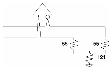
The video data and control signals are transmitted from MC100E151 registers clocked by the rising edge of pixel clock. The data signals must be terminated at the receiver with the Thevinin-equivalent network shown in Figure 1-3. The DVP interface is a point-to-point interface.
| Note: Do not bus the signals. The cable has a 110-ohm characteristic impedance, and is designed to be used with PC boards of 55-ohm characteristic impedance traces. Be sure that all data signal pairs are of equal length, and as short as possible. Terminations should be at the end-of-line, within 300 mils of the differential receiver inputs. |
DVP pixel clock can be programmed to operate between 2.5 MHz and 175 MHz, allowing the DVP interface to support video formats between 2.5 and 175 Mpix/sec. (The DVP board was designed for a maximum operating rate of 230 Mpixels/sec, but is not guaranteed beyond 175 Mpix/sec in the Onyx InfiniteReality graphics system. Contact Silicon Graphics if your application requirements exceed 175 Mpixels/sec.)
Over most of the DVP's operating range, clock skew is an important consideration in the transmission of pixel clock to the video option board and distributing it to the video option board. Because of its wide operating limits, phase-locked-loop techniques are unsuitable for receiving the clocks on the DVP interface. Figure 1-4 shows the circuit recommended by Silicon Graphics for receiving and regenerating a full-speed pixel clock, the method of distributing it, and the recommended circuits for receiving DVP video data. The recommended data receiver is a Motorola MC100E452. The recommended clock receiver is a Synergy Semiconductor SY100EL16A.
When the external DVP interface cable is not in place, the data drivers are powered down to save power and minimize EMI interference to other equipment. 5V-PECL signals have lower emissions than CMOS or TTL signals. Each differential pair in the external cable is individually shielded with foil. In addition, the entire cable is shielded with a braided shield. The external shield of the DVP cable must be tied directly to chassis ground on both the Silicon Graphics logic cabinet and the customer's chassis.
Chassis grounds (on the Onyx rack and the customer equipment) should be at the same potentials, supplied from the same AC mains and ground. PWR_GOOD is likely to be out of spec if there is much difference in ground potential between the two equipment chassis, resulting in a shutdown of the DVP interface to prevent equipment damage. (See “Receiver Power Indicator (PWR_GOOD)” for more information.) Both chassis should be supplied from the same AC electrical source in order to minimize ground differentials between chassis.
 | Caution: Any difference in ground potential greater than 500 millivolts (0.5 volts) between two chassis connected by copper XIO cables can cause severe equipment damage, and can create hazardous conditions. |
The branch circuit wiring should be provided with an insulated grounding conductor that is identical in size, insulation material, and thickness to the earthed and unearthed branch-circuit supply conductors. The grounding conductor should be green, with or without one or more yellow stripes. This grounding or earthing conductor should be connected to earth at the service equipment or, if supplied by a separately derived system, at the supply transformer or motor-generated set. The power receptacles in the vicinity of the systems should all be of an earthing type, and the grounding or earthing conductors serving these receptacles should be connected to earth at the service equipment.
To access 16-bit luminance (high-resolution monochrome) using the DVP interface, the application program must open a 16-bit luminance X-Windows visual. When this is done, the DVP interface presents the 12 MSBs of luminance on the RED_OUT_{H,L}[11:0] and (redundantly) on GREEN_OUT_{H,L}[11:0] bits. The 4 LSBs are contained on the BLUE_OUT_{H,L}[3:0] bits. BLUE_OUT_{H,L}[11:4] contain another redundant copy of the 8 MSBs of luminance. This provides access to 16-bit luminance without interfering with the monochrome display of luminance on 8-bit-per-component analog video channels, since all three color channels contain the 8 MSBs of luminance.
When considering applications of 16-bit luminance, remember that the InfiniteReality implementation of OpenGL does not support 16-bit rendering such as lighting and shading. However, 16-bit texturing is fully supported.
The DVP can accommodate custom video formats, if needed. InfiniteReality graphics supports flexible, user-programmable video formats. As previously mentioned, the DVP supports the full range of pixel clock rates available in the InfiniteReality graphics subsystem. To load and run video formats on DVP, use the ircombine tool. For more information about the Video Format Compiler and the ircombine tool, see the Video Format Compiler Programming Manual (Silicon Graphics part number 007-3402-001), and the IRcombine User Manual (Silicon Graphics part number 007-3279-001).
The DVP appears as another video channel in the ircombine tool's user interface. Use of the DVP does not disable any other video channel. However, the rules for combining video formats to run on multiple channels (e.g., total memory and video bandwidth must not be exceeded; swap-rates must match across channels) apply to DVP as they do to the analog video channels.
The equipment connected to the DVP interface is expected to be slaved to the video timing of the DG4 board via the DVP signals FRAME_{H,L}, VSYNC_{H,L}, CSYNC_{H,L}, and CBLANK_{H,L}. Operating the receiver in slave mode results in the absolute minimum video data latency.
In certain applications, the DG4 video output can be slaved to the external equipment. This should be done using the DG4 external frame-locking facility. (See DG4 documentation for more information.) The horizontal phase adjustment of DG4 genlock circuits can be used to adjust for delays in cabling and equipment. However, the user is cautioned against expecting pixel- or sub-pixel accuracy. In most cases, such accuracy is not necessary. The receiving equipment may require FIFO memories to receive video data in order to operate reliably in this mode. These FIFO memories may increase the latency of the DVP video channel depending on their depth. Proper consideration of these important design issues in the early stages of the receiver design will avoid unforeseen problems later on.
Table 1-1 shows the signals on the DVIO connector.
Table 1-1. DVP Transmitter (DVIO) Pinouts
Pin No. | Pin Name |
|---|---|
MTG1 | CHASSIS_GND |
1 | RED_OUT_H[11] |
2 | RED_OUT_L[11] |
3 | RED_OUT_H[10] |
4 | RED_OUT_L[10] |
5 | RED_OUT_H[9] |
6 | RED_OUT_L[9] |
7 | RED_OUT_H[8] |
8 | RED_OUT_L[8] |
9 | RED_OUT_H[7] |
10 | RED_OUT_L[7] |
11 | RED_OUT_H[6] |
12 | RED_OUT_L[6] |
13 | RED_OUT_H[5] |
14 | RED_OUT_L[5] |
15 | RED_OUT_H[4] |
16 | RED_OUT_L[4] |
17 | RED_OUT_H[3] |
18 | RED_OUT_L[3] |
19 | RED_OUT_H[2] |
20 | RED_OUT_L[2] |
21 | RED_OUT_H[1] |
22 | RED_OUT_L[1] |
23 | RED_OUT_H[0] |
24 | RED_OUT_L[0] |
25 | PWR_GOOD |
26 | GND |
27 | GREEN_OUT_H[11] |
28 | GREEN_OUT_L[11] |
29 | GREEN_OUT_H[10 |
30 | GREEN_OUT_L[10] |
31 | GREEN_OUT_H[9] |
32 | GREEN_OUT_L[9] |
33 | GREEN_OUT_H[8] |
34 | GREEN_OUT_L[8] |
35 | GREEN_OUT_H[7] |
36 | GREEN_OUT_L[7] |
37 | GREEN_OUT_H[6] |
38 | GREEN_OUT_L[6] |
39 | GREEN_OUT_H[5] |
40 | GREEN_OUT_L[5] |
41 | GREEN_OUT_H[4] |
42 | GREEN_OUT_L[4] |
43 | GREEN_OUT_H[3] |
44 | GREEN_OUT_L[3] |
45 | GREEN_OUT_H[2] |
46 | GREEN_OUT_L[2] |
47 | GREEN_OUT_H[1] |
48 | GREEN_OUT_L[1] |
49 | GREEN_OUT_H[0] |
50 | GREEN_OUT_L[0] |
51 | BLUE_OUT_H[11] |
52 | BLUE_OUT_L[11] |
53 | BLUE_OUT_H[10] |
54 | BLUE_OUT_L[10] |
55 | BLUE_OUT_H[9] |
56 | BLUE_OUT_L[9] |
57 | BLUE_OUT_H[8] |
58 | BLUE_OUT_L[8] |
59 | BLUE_OUT_H[7] |
60 | BLUE_OUT_L[7] |
61 | BLUE_OUT_H[6] |
62 | BLUE_OUT_L[6] |
63 | BLUE_OUT_H[5] |
64 | BLUE_OUT_L[5] |
65 | BLUE_OUT_H[4] |
66 | BLUE_OUT_L[4] |
67 | BLUE_OUT_H[3] |
68 | BLUE_OUT_L[3] |
69 | BLUE_OUT_H[2] |
70 | BLUE_OUT_L[2] |
71 | BLUE_OUT_H[1] |
72 | BLUE_OUT_L[1] |
73 | BLUE_OUT_H[0] |
74 | BLUE_OUT_L[0] |
75 | I2C_DATA |
76 | I2C_DATA_GND |
77 | I2C_CLK |
78 | I2C_CLK_GND |
79 | CBLANK_H |
80 | CBLANK_L |
81 | CSYNC_H |
82 | CSYNC_L |
83 | VSYNC_H |
84 | VSYNC_L |
85 | FIELD_H |
86 | FIELD_L |
87 | VOC_SWAP_H |
88 | VOC_SWAP_L |
89 | HMUX_SEL1_H |
90 | HMUX_SEL1_L |
91 | HMUX_SEL0_H |
92 | HMUX_SEL0_L |
93 | GND |
94 | GND |
95 | CLK_2_H |
96 | CLK_2_L |
97 | GND |
98 | GND |
99 | CLK_2_QUAD_H |
100 | CLK_2_QUAD_L |
MTG2 | CHASSIS_GND |
Because of the construction of the external cable, the pinout is reversed on the receiver connector. Table 1-2 shows the pinout of the receiver connector.
Table 1-2. DVP Receiver Pinouts
Pin No. | Pin Name |
|---|---|
MTG1 | CHASSIS_GND |
1 | CLK_2_QUAD_L |
2 | CLK_2_QUAD_H |
3 | GND |
4 | GND |
5 | CLK_2_L |
6 | CLK_2_H |
7 | GND |
8 | GND |
9 | HMUX_SEL0_L |
10 | HMUX_SEL0_H |
11 | HMUX_SEL1_L |
12 | HMUX_SEL1_H |
13 | VOC_SWAP_L |
14 | VOC_SWAP_H |
15 | FIELD_L |
16 | FIELD_H |
17 | VSYNC_L |
18 | VSYNC_H |
19 | CSYNC_L |
20 | CSYNC_H |
21 | CBLANK_L |
22 | CBLANK_H |
23 | I2C_CLK_GND |
24 | I2C_CLK |
25 | I2C_DATA_GND |
26 | I2C_DATA |
27 | BLUE_OUT_L[0] |
28 | BLUE_OUT_H[0] |
29 | BLUE_OUT_L[1] |
30 | BLUE_OUT_H[1] |
31 | BLUE_OUT_L[2] |
32 | BLUE_OUT_H[2] |
33 | BLUE_OUT_L[3] |
34 | BLUE_OUT_H[3] |
35 | BLUE_OUT_L[4] |
36 | BLUE_OUT_H[4] |
37 | BLUE_OUT_L[5] |
38 | BLUE_OUT_H[5] |
39 | BLUE_OUT_L[6] |
40 | BLUE_OUT_H[6] |
41 | BLUE_OUT_L[7] |
42 | BLUE_OUT_H[7] |
43 | BLUE_OUT_L[8] |
44 | BLUE_OUT_H[8] |
45 | BLUE_OUT_L[9] |
46 | BLUE_OUT_H[9] |
47 | BLUE_OUT_L[10] |
48 | BLUE_OUT_H[10] |
49 | BLUE_OUT_L[11] |
50 | BLUE_OUT_H[11] |
51 | GREEN_OUT_L[0] |
52 | GREEN_OUT_H[0] |
53 | GREEN_OUT_L[1] |
54 | GREEN_OUT_H[1] |
55 | GREEN_OUT_L[2] |
56 | GREEN_OUT_H[2] |
57 | GREEN_OUT_L[3] |
58 | GREEN_OUT_H[3] |
59 | GREEN_OUT_L[4] |
60 | GREEN_OUT_H[4] |
61 | GREEN_OUT_L[5] |
62 | GREEN_OUT_H[5] |
63 | GREEN_OUT_L[6] |
64 | GREEN_OUT_H[6] |
65 | GREEN_OUT_L[7] |
66 | GREEN_OUT_H[7] |
67 | GREEN_OUT_L[8] |
68 | GREEN_OUT_H[8] |
69 | GREEN_OUT_L[9] |
70 | GREEN_OUT_H[9] |
71 | GREEN_OUT_L[10] |
72 | GREEN_OUT_H[10] |
73 | GREEN_OUT_L[11] |
74 | GREEN_OUT_H[11] |
75 | GND |
76 | PWR_GOOD |
77 | RED_OUT_L[0] |
78 | RED_OUT_H[0] |
79 | RED_OUT_L[1] |
80 | RED_OUT_H[1] |
81 | RED_OUT_L[2] |
82 | RED_OUT_H[2] |
83 | RED_OUT_L[3] |
84 | RED_OUT_H[3] |
85 | RED_OUT_L[4] |
86 | RED_OUT_H[4] |
87 | RED_OUT_L[5] |
88 | RED_OUT_H[5] |
89 | RED_OUT_L[6] |
90 | RED_OUT_H[6] |
91 | RED_OUT_L[7] |
92 | RED_OUT_H[7] |
93 | RED_OUT_L[8] |
94 | RED_OUT_H[8] |
95 | RED_OUT_L[9] |
96 | RED_OUT_H[9] |
97 | RED_OUT_L[10] |
98 | RED_OUT_H[10] |
99 | RED_OUT_L[11] |
100 | RED_OUT_H[11] |
MTG2 | CHASSIS_GND |